

6.7 Methods of Counteracting Microcircuit Re-engineering Processes
611
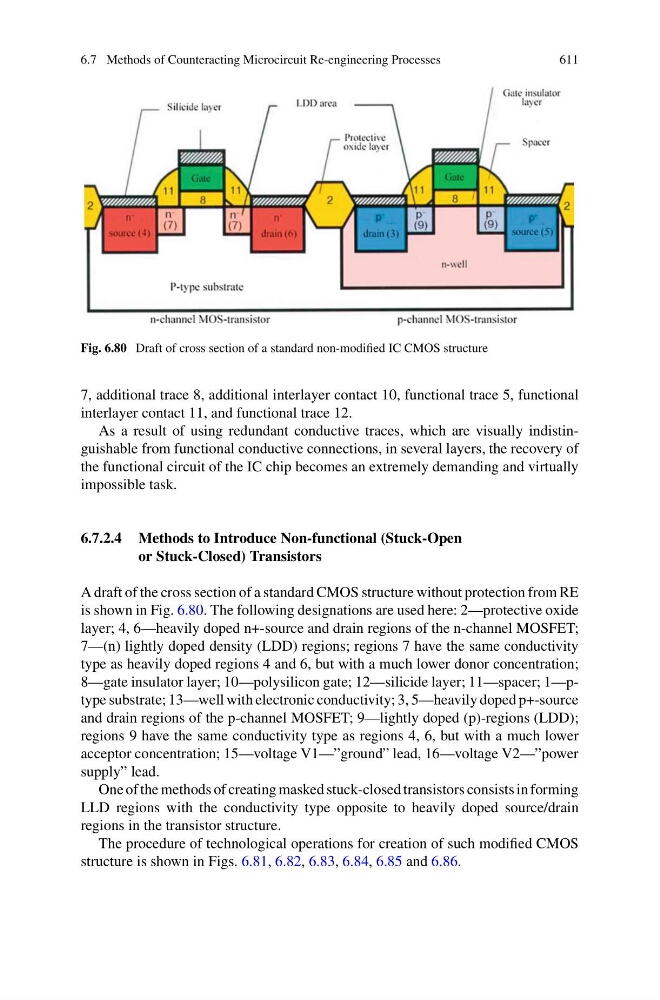
Fig. 6.80 Draft of cross section of a standard non-modified IC CMOS structure
7, additional trace 8, additional interlayer contact 10, functional trace 5, functional
interlayer contact 11, and functional trace 12.
As a result of using redundant conductive traces, which are visually indistinguishable from functional conductive connections, in several layers, the recovery of
the functional circuit of the IC chip becomes an extremely demanding and virtually
impossible task.
6.7.2.4 Methods to Introduce Non-functional (Stuck-Open
or Stuck-Closed) Transistors
A draft of the cross section of a standard CMOS structure without protection from RE
is shown in Fig. 6.80. The following designations are used here: 2—protective oxide
layer; 4, 6—heavily doped n+-source and drain regions of the n-channel MOSFET;
7—(n) lightly doped density (LDD) regions; regions 7 have the same conductivity
type as heavily doped regions 4 and 6, but with a much lower donor concentration;
8—gate insulator layer; 10—polysilicon gate; 12—silicide layer; 11—spacer; 1—ptype substrate; 13—well with electronic conductivity; 3, 5—heavily doped p+-source
and drain regions of the p-channel MOSFET; 9—lightly doped (p)-regions (LDD);
regions 9 have the same conductivity type as regions 4, 6, but with a much lower
acceptor concentration; 15—voltage V1—”ground” lead, 16—voltage V2—”power
supply” lead.
One of the methods of creating masked stuck-closed transistors consists in forming
LLD regions with the conductivity type opposite to heavily doped source/drain
regions in the transistor structure.
The procedure of technological operations for creation of such modified CMOS
structure is shown in Figs. 6.81, 6.82, 6.83, 6.84, 6.85 and 6.86.
611
Fig. 6.80 Draft of cross section of a standard non-modified IC CMOS structure
7, additional trace 8, additional interlayer contact 10, functional trace 5, functional
interlayer contact 11, and functional trace 12.
As a result of using redundant conductive traces, which are visually indistinguishable from functional conductive connections, in several layers, the recovery of
the functional circuit of the IC chip becomes an extremely demanding and virtually
impossible task.
6.7.2.4 Methods to Introduce Non-functional (Stuck-Open
or Stuck-Closed) Transistors
A draft of the cross section of a standard CMOS structure without protection from RE
is shown in Fig. 6.80. The following designations are used here: 2—protective oxide
layer; 4, 6—heavily doped n+-source and drain regions of the n-channel MOSFET;
7—(n) lightly doped density (LDD) regions; regions 7 have the same conductivity
type as heavily doped regions 4 and 6, but with a much lower donor concentration;
8—gate insulator layer; 10—polysilicon gate; 12—silicide layer; 11—spacer; 1—ptype substrate; 13—well with electronic conductivity; 3, 5—heavily doped p+-source
and drain regions of the p-channel MOSFET; 9—lightly doped (p)-regions (LDD);
regions 9 have the same conductivity type as regions 4, 6, but with a much lower
acceptor concentration; 15—voltage V1—”ground” lead, 16—voltage V2—”power
supply” lead.
One of the methods of creating masked stuck-closed transistors consists in forming
LLD regions with the conductivity type opposite to heavily doped source/drain
regions in the transistor structure.
The procedure of technological operations for creation of such modified CMOS
structure is shown in Figs. 6.81, 6.82, 6.83, 6.84, 6.85 and 6.86.