

6.6 Methods of Preparing Samples of Submicron Microcircuits …
601
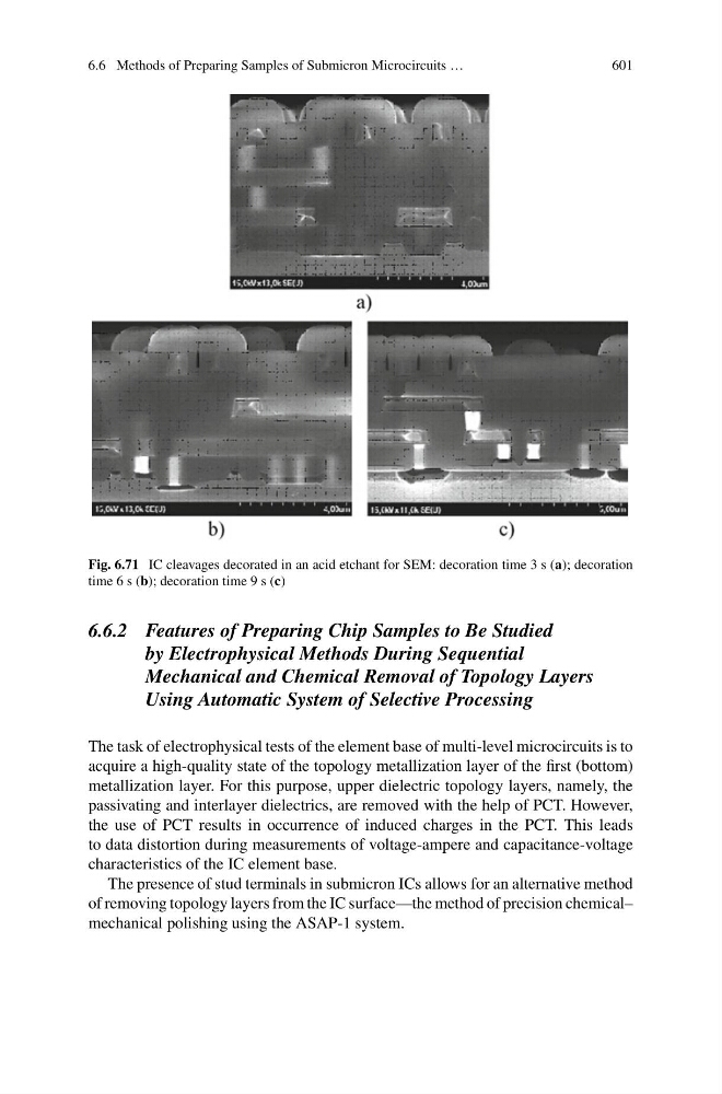
Fig. 6.71 IC cleavages decorated in an acid etchant for SEM: decoration time 3 s (a); decoration
time 6 s (b); decoration time 9 s (c)
6.6.2 Features of Preparing Chip Samples to Be Studied
by Electrophysical Methods During Sequential
Mechanical and Chemical Removal of Topology Layers
Using Automatic System of Selective Processing
The task of electrophysical tests of the element base of multi-level microcircuits is to
acquire a high-quality state of the topology metallization layer of the first (bottom)
metallization layer. For this purpose, upper dielectric topology layers, namely, the
passivating and interlayer dielectrics, are removed with the help of PCT. However,
the use of PCT results in occurrence of induced charges in the PCT. This leads
to data distortion during measurements of voltage-ampere and capacitance-voltage
characteristics of the IC element base.
The presence of stud terminals in submicron ICs allows for an alternative method
of removing topology layers from the IC surface—the method of precision chemical–
mechanical polishing using the ASAP-1 system.
601
Fig. 6.71 IC cleavages decorated in an acid etchant for SEM: decoration time 3 s (a); decoration
time 6 s (b); decoration time 9 s (c)
6.6.2 Features of Preparing Chip Samples to Be Studied
by Electrophysical Methods During Sequential
Mechanical and Chemical Removal of Topology Layers
Using Automatic System of Selective Processing
The task of electrophysical tests of the element base of multi-level microcircuits is to
acquire a high-quality state of the topology metallization layer of the first (bottom)
metallization layer. For this purpose, upper dielectric topology layers, namely, the
passivating and interlayer dielectrics, are removed with the help of PCT. However,
the use of PCT results in occurrence of induced charges in the PCT. This leads
to data distortion during measurements of voltage-ampere and capacitance-voltage
characteristics of the IC element base.
The presence of stud terminals in submicron ICs allows for an alternative method
of removing topology layers from the IC surface—the method of precision chemical–
mechanical polishing using the ASAP-1 system.