

6.4 Complex Methodology for Reverse Engineering …
549
Table 6.1 (continued)
Microscopical method
Resolution
features and
description
Morphological-topological image of
an IC chip fragment
High resolution
less than 1 nm,
small scanning
field,
restriction on
the height of
the relief
Atomic force microscopy
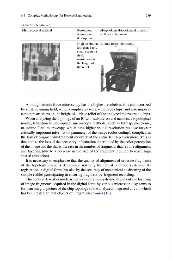
Although atomic force microscopy has the highest resolution, it is characterized
by small scanning field, which complicates work with large chips, and also imposes
certain restrictions on the height of surface relief of the analyzed microcircuit chips.
When analyzing the topology of an IC with submicron and nanoscale topological
norms, transition to non-optical microscopy methods, such as bitmap, electronic,
or atomic force microscopy, which have higher spatial resolution but lose another
critically important information parameter of the image (color coding), complicates
the task of fragment-by-fragment recovery of the entire IC chip even more. This is
due both to the loss of the necessary information determined by the color perception
of the image and the sharp increase in the number of fragments that require alignment
and layering (due to a decrease in the size of the fragment required to reach high
spatial resolution).
It is necessary to emphasize that the quality of alignment of separate fragments
of the topology image is determined not only by optical or probe system of its
registration in digital form, but also by the accuracy of mechanical positioning of the
sample (table) participating in ensuring fragment-by-fragment recording.
This section describes modern methods of frame-by-frame alignment and layering
of image fragments acquired in the digital form by various microscopic systems to
form an integral picture of the chip topology of the analyzed integrated circuit, which
has been tested on real objects of integral electronics [10].
549
Table 6.1 (continued)
Microscopical method
Resolution
features and
description
Morphological-topological image of
an IC chip fragment
High resolution
less than 1 nm,
small scanning
field,
restriction on
the height of
the relief
Atomic force microscopy
Although atomic force microscopy has the highest resolution, it is characterized
by small scanning field, which complicates work with large chips, and also imposes
certain restrictions on the height of surface relief of the analyzed microcircuit chips.
When analyzing the topology of an IC with submicron and nanoscale topological
norms, transition to non-optical microscopy methods, such as bitmap, electronic,
or atomic force microscopy, which have higher spatial resolution but lose another
critically important information parameter of the image (color coding), complicates
the task of fragment-by-fragment recovery of the entire IC chip even more. This is
due both to the loss of the necessary information determined by the color perception
of the image and the sharp increase in the number of fragments that require alignment
and layering (due to a decrease in the size of the fragment required to reach high
spatial resolution).
It is necessary to emphasize that the quality of alignment of separate fragments
of the topology image is determined not only by optical or probe system of its
registration in digital form, but also by the accuracy of mechanical positioning of the
sample (table) participating in ensuring fragment-by-fragment recording.
This section describes modern methods of frame-by-frame alignment and layering
of image fragments acquired in the digital form by various microscopic systems to
form an integral picture of the chip topology of the analyzed integrated circuit, which
has been tested on real objects of integral electronics [10].