

548
6 Reverse Engineering of Microcircuits
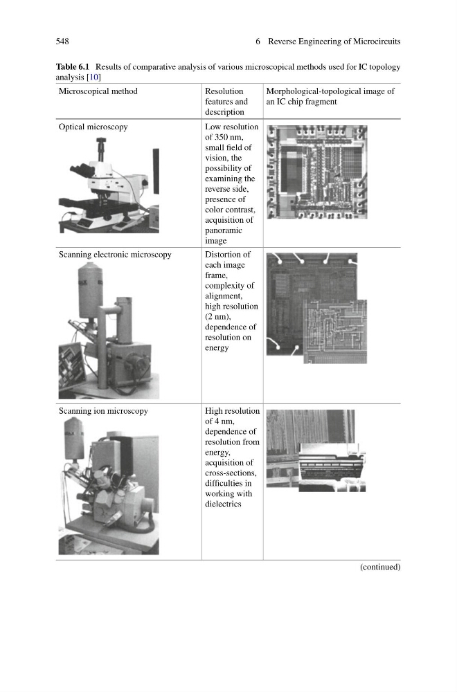
Table 6.1 Results of comparative analysis of various microscopical methods used for IC topology
analysis [10]
Microscopical method
Resolution
features and
description
Morphological-topological image of
an IC chip fragment
Optical microscopy
Low resolution
of 350 nm,
small field of
vision, the
possibility of
examining the
reverse side,
presence of
color contrast,
acquisition of
panoramic
image
Scanning electronic microscopy
Distortion of
each image
frame,
complexity of
alignment,
high resolution
(2 nm),
dependence of
resolution on
energy
Scanning ion microscopy
High resolution
of 4 nm,
dependence of
resolution from
energy,
acquisition of
cross-sections,
difficulties in
working with
dielectrics
(continued)
6 Reverse Engineering of Microcircuits
Table 6.1 Results of comparative analysis of various microscopical methods used for IC topology
analysis [10]
Microscopical method
Resolution
features and
description
Morphological-topological image of
an IC chip fragment
Optical microscopy
Low resolution
of 350 nm,
small field of
vision, the
possibility of
examining the
reverse side,
presence of
color contrast,
acquisition of
panoramic
image
Scanning electronic microscopy
Distortion of
each image
frame,
complexity of
alignment,
high resolution
(2 nm),
dependence of
resolution on
energy
Scanning ion microscopy
High resolution
of 4 nm,
dependence of
resolution from
energy,
acquisition of
cross-sections,
difficulties in
working with
dielectrics
(continued)