

534
6 Reverse Engineering of Microcircuits
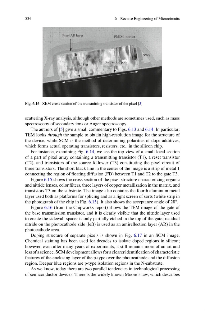
Fig. 6.16 XEM cross section of the transmitting transistor of the pixel [5]
scattering X-ray analysis, although other methods are sometimes used, such as mass
spectroscopy of secondary ions or Auger spectroscopy.
The authors of [5] give a small commentary to Figs. 6.13 and 6.14. In particular:
TEM looks through the sample to obtain high-resolution image for the structure of
the device, while SCM is the method of determining polarities of dope additives,
which forms actual operating transistors, resistors, etc., in the silicon chip.
For instance, examining Fig. 6.14, we see the top view of a small local section
of a part of pixel array containing a transmitting transistor (T1), a reset transistor
(T2), and transistors of the source follower (T3) constituting the pixel circuit of
three transistors. The short black line in the center of the image is a strip of metal 1
connecting the region of floating diffusion (FD) between T1 and T2 to the gate T3.
Figure 6.15 shows the cross section of the pixel structure characterizing organic
and nitride lenses, color filters, three layers of copper metallization in the matrix, and
transistors T3 on the substrate. The image also contains the fourth aluminum metal
layer used both as platforms for splicing and as a light screen of sorts (white strip in
the photograph of the chip in Fig. 6.15). It also shows the acceptance angle of 28°.
Figure 6.16 (from the Chipworks report) shows the TEM image of the gate of
the base transmission transistor, and it is clearly visible that the nitride layer used
to create the sidewall spacer is only partially etched in the top of the gate; residual
nitride on the photocathode side (left) is used as an antireflection layer (AR) in the
photocathode area.
Doping structure of separate pixels is shown in Fig. 6.17 in an SCM image.
Chemical staining has been used for decades to isolate doped regions in silicon;
however, even after many years of experiments, it still remains more of an art and
less of a science. SCM development allows for a clearer identification of characteristic
features of the enclosing layer of the p-type over the photocathode and the diffusion
region. Deeper blue regions are p-type isolation regions in the N-substrate.
As we know, today there are two parallel tendencies in technological processing
of semiconductor devices. There is the widely known Moore’s law, which describes
6 Reverse Engineering of Microcircuits
Fig. 6.16 XEM cross section of the transmitting transistor of the pixel [5]
scattering X-ray analysis, although other methods are sometimes used, such as mass
spectroscopy of secondary ions or Auger spectroscopy.
The authors of [5] give a small commentary to Figs. 6.13 and 6.14. In particular:
TEM looks through the sample to obtain high-resolution image for the structure of
the device, while SCM is the method of determining polarities of dope additives,
which forms actual operating transistors, resistors, etc., in the silicon chip.
For instance, examining Fig. 6.14, we see the top view of a small local section
of a part of pixel array containing a transmitting transistor (T1), a reset transistor
(T2), and transistors of the source follower (T3) constituting the pixel circuit of
three transistors. The short black line in the center of the image is a strip of metal 1
connecting the region of floating diffusion (FD) between T1 and T2 to the gate T3.
Figure 6.15 shows the cross section of the pixel structure characterizing organic
and nitride lenses, color filters, three layers of copper metallization in the matrix, and
transistors T3 on the substrate. The image also contains the fourth aluminum metal
layer used both as platforms for splicing and as a light screen of sorts (white strip in
the photograph of the chip in Fig. 6.15). It also shows the acceptance angle of 28°.
Figure 6.16 (from the Chipworks report) shows the TEM image of the gate of
the base transmission transistor, and it is clearly visible that the nitride layer used
to create the sidewall spacer is only partially etched in the top of the gate; residual
nitride on the photocathode side (left) is used as an antireflection layer (AR) in the
photocathode area.
Doping structure of separate pixels is shown in Fig. 6.17 in an SCM image.
Chemical staining has been used for decades to isolate doped regions in silicon;
however, even after many years of experiments, it still remains more of an art and
less of a science. SCM development allows for a clearer identification of characteristic
features of the enclosing layer of the p-type over the photocathode and the diffusion
region. Deeper blue regions are p-type isolation regions in the N-substrate.
As we know, today there are two parallel tendencies in technological processing
of semiconductor devices. There is the widely known Moore’s law, which describes