

6.3 Basics of Reverse-Engineering Art
535
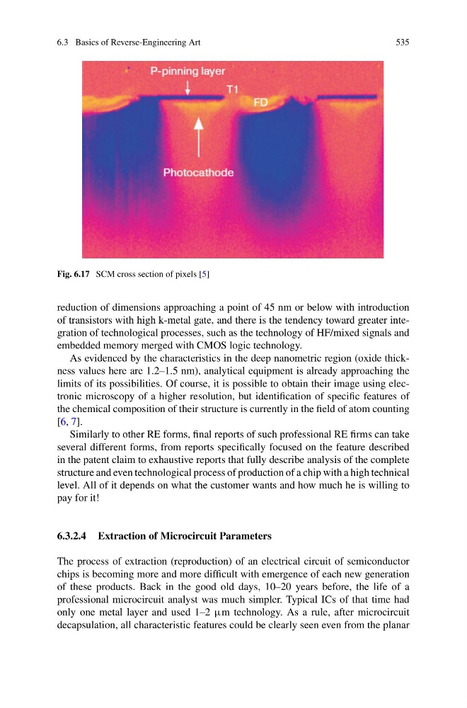
Fig. 6.17 SCM cross section of pixels [5]
reduction of dimensions approaching a point of 45 nm or below with introduction
of transistors with high k-metal gate, and there is the tendency toward greater integration of technological processes, such as the technology of HF/mixed signals and
embedded memory merged with CMOS logic technology.
As evidenced by the characteristics in the deep nanometric region (oxide thickness values here are 1.2–1.5 nm), analytical equipment is already approaching the
limits of its possibilities. Of course, it is possible to obtain their image using electronic microscopy of a higher resolution, but identification of specific features of
the chemical composition of their structure is currently in the field of atom counting
[6, 7].
Similarly to other RE forms, final reports of such professional RE firms can take
several different forms, from reports specifically focused on the feature described
in the patent claim to exhaustive reports that fully describe analysis of the complete
structure and even technological process of production of a chip with a high technical
level. All of it depends on what the customer wants and how much he is willing to
pay for it!
6.3.2.4 Extraction of Microcircuit Parameters
The process of extraction (reproduction) of an electrical circuit of semiconductor
chips is becoming more and more difficult with emergence of each new generation
of these products. Back in the good old days, 10–20 years before, the life of a
professional microcircuit analyst was much simpler. Typical ICs of that time had
only one metal layer and used 1–2 μm technology. As a rule, after microcircuit
decapsulation, all characteristic features could be clearly seen even from the planar
535
Fig. 6.17 SCM cross section of pixels [5]
reduction of dimensions approaching a point of 45 nm or below with introduction
of transistors with high k-metal gate, and there is the tendency toward greater integration of technological processes, such as the technology of HF/mixed signals and
embedded memory merged with CMOS logic technology.
As evidenced by the characteristics in the deep nanometric region (oxide thickness values here are 1.2–1.5 nm), analytical equipment is already approaching the
limits of its possibilities. Of course, it is possible to obtain their image using electronic microscopy of a higher resolution, but identification of specific features of
the chemical composition of their structure is currently in the field of atom counting
[6, 7].
Similarly to other RE forms, final reports of such professional RE firms can take
several different forms, from reports specifically focused on the feature described
in the patent claim to exhaustive reports that fully describe analysis of the complete
structure and even technological process of production of a chip with a high technical
level. All of it depends on what the customer wants and how much he is willing to
pay for it!
6.3.2.4 Extraction of Microcircuit Parameters
The process of extraction (reproduction) of an electrical circuit of semiconductor
chips is becoming more and more difficult with emergence of each new generation
of these products. Back in the good old days, 10–20 years before, the life of a
professional microcircuit analyst was much simpler. Typical ICs of that time had
only one metal layer and used 1–2 μm technology. As a rule, after microcircuit
decapsulation, all characteristic features could be clearly seen even from the planar