

42
G. K. Ananthasuresh
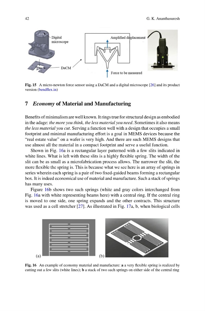
Fig. 15 A micro-newton force sensor using a DaCM and a digital microscope [26] and its product
version (bendflex.in)
7 Economy of Material and Manufacturing
Benefits of minimalism are well known. It rings true for structural design as embodied
in the adage: the more you think, the less material you need. Sometimes it also means
the less material you cut. Serving a function well with a design that occupies a small
footprint and minimal manufacturing effort is a goal in MEMS devices because the
“real estate value” on a wafer is very high. And there are such MEMS designs that
use almost all the material in a compact footprint and serve a useful function.
Shown in Fig. 16a is a rectangular layer patterned with a few slits indicated in
white lines. What is left with these slits is a highly flexible spring. The width of the
slit can be as small as a microfabrication process allows. The narrower the slit, the
more flexible the spring is. This is because what we see here is an array of springs in
series wherein each spring is a pair of two fixed-guided beams forming a rectangular
box. It is indeed economical use of material and manufacture. Such a stack of springs
has many uses.
Figure 16b shows two such springs (white and gray colors interchanged from
Fig. 16a with white representing beams here) with a central ring. If the central ring
is moved to one side, one spring expands and the other contracts. This structure
was used as a cell stretcher [27]. As illustrated in Fig. 17a, b, when biological cells
Fig. 16 An example of economy material and manufacture: a a very flexible spring is realized by
cutting out a few slits (white lines); b a stack of two such springs on either side of the central ring
G. K. Ananthasuresh
Fig. 15 A micro-newton force sensor using a DaCM and a digital microscope [26] and its product
version (bendflex.in)
7 Economy of Material and Manufacturing
Benefits of minimalism are well known. It rings true for structural design as embodied
in the adage: the more you think, the less material you need. Sometimes it also means
the less material you cut. Serving a function well with a design that occupies a small
footprint and minimal manufacturing effort is a goal in MEMS devices because the
“real estate value” on a wafer is very high. And there are such MEMS designs that
use almost all the material in a compact footprint and serve a useful function.
Shown in Fig. 16a is a rectangular layer patterned with a few slits indicated in
white lines. What is left with these slits is a highly flexible spring. The width of the
slit can be as small as a microfabrication process allows. The narrower the slit, the
more flexible the spring is. This is because what we see here is an array of springs in
series wherein each spring is a pair of two fixed-guided beams forming a rectangular
box. It is indeed economical use of material and manufacture. Such a stack of springs
has many uses.
Figure 16b shows two such springs (white and gray colors interchanged from
Fig. 16a with white representing beams here) with a central ring. If the central ring
is moved to one side, one spring expands and the other contracts. This structure
was used as a cell stretcher [27]. As illustrated in Fig. 17a, b, when biological cells
Fig. 16 An example of economy material and manufacture: a a very flexible spring is realized by
cutting out a few slits (white lines); b a stack of two such springs on either side of the central ring