

9 Emerging Hardware Technologies for IoT Data Processing
437
neous computers have been proposed that integrate more than one kind of processing
core, each of which optimized for accelerating certain tasks. The main objectives in
heterogeneous computing are (1) to enhance the application development through
a seamless and flexible programing interface and (2) to improve the performance
and energy-efficiency of the user applications by executing parts of the code
on dedicated hardware. For example, consider a coprocessing architecture that
comprises a central processing unit (CPU) to realize complex serial tasks, such
as the sine function, and a graphics processing unit (GPU) that is specifically
designed for accelerating massively data-parallel operations, such as pixel and
vector processing. Other types of processing units, such as digital processing
unit (DSP), field-programmable gate array (FPGA), and deep neural network
(DNN) accelerators, are examples of popular technologies used for heterogeneous
computing. A key challenge in designing heterogeneous computers is to strike a
balance between the expected performance potentials and the cost of integrating
disparate technologies. Typically, an ideal balance between cost and versatility may
only be achieved if the heterogeneous cores require a minimal complexity and
overhead for communication.
9.2.2 In-Package Die Stacking
One of the key solutions to the bandwidth and energy-efficiency problems is to
reduce the high cost of data movement in computer systems. Minimizing the high
cost of data movement in computing systems has been the main motivation for the
recent innovations in 3D die stacking of silicon dice with disparate technologies
within the same package. The 3D stacking technology has enabled energy-efficient
solutions for near-data processing by integrating multiple dice of high-density
memory layers and processor cores within the same package to amortize the high
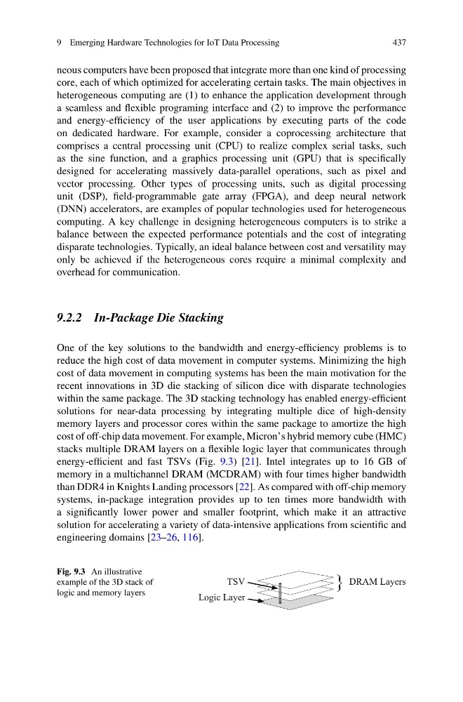
cost of off-chip data movement. For example, Micron’s hybrid memory cube (HMC)
stacks multiple DRAM layers on a flexible logic layer that communicates through
energy-efficient and fast TSVs (Fig. 9.3) [21]. Intel integrates up to 16 GB of
memory in a multichannel DRAM (MCDRAM) with four times higher bandwidth
than DDR4 in Knights Landing processors [22]. As compared with off-chip memory
systems, in-package integration provides up to ten times more bandwidth with
a significantly lower power and smaller footprint, which make it an attractive
solution for accelerating a variety of data-intensive applications from scientific and
engineering domains [23–26, 116].
Fig. 9.3 An illustrative
example of the 3D stack of
logic and memory layers
Logic Layer
DRAM Layers
}
TSV
437
neous computers have been proposed that integrate more than one kind of processing
core, each of which optimized for accelerating certain tasks. The main objectives in
heterogeneous computing are (1) to enhance the application development through
a seamless and flexible programing interface and (2) to improve the performance
and energy-efficiency of the user applications by executing parts of the code
on dedicated hardware. For example, consider a coprocessing architecture that
comprises a central processing unit (CPU) to realize complex serial tasks, such
as the sine function, and a graphics processing unit (GPU) that is specifically
designed for accelerating massively data-parallel operations, such as pixel and
vector processing. Other types of processing units, such as digital processing
unit (DSP), field-programmable gate array (FPGA), and deep neural network
(DNN) accelerators, are examples of popular technologies used for heterogeneous
computing. A key challenge in designing heterogeneous computers is to strike a
balance between the expected performance potentials and the cost of integrating
disparate technologies. Typically, an ideal balance between cost and versatility may
only be achieved if the heterogeneous cores require a minimal complexity and
overhead for communication.
9.2.2 In-Package Die Stacking
One of the key solutions to the bandwidth and energy-efficiency problems is to
reduce the high cost of data movement in computer systems. Minimizing the high
cost of data movement in computing systems has been the main motivation for the
recent innovations in 3D die stacking of silicon dice with disparate technologies
within the same package. The 3D stacking technology has enabled energy-efficient
solutions for near-data processing by integrating multiple dice of high-density
memory layers and processor cores within the same package to amortize the high
cost of off-chip data movement. For example, Micron’s hybrid memory cube (HMC)
stacks multiple DRAM layers on a flexible logic layer that communicates through
energy-efficient and fast TSVs (Fig. 9.3) [21]. Intel integrates up to 16 GB of
memory in a multichannel DRAM (MCDRAM) with four times higher bandwidth
than DDR4 in Knights Landing processors [22]. As compared with off-chip memory
systems, in-package integration provides up to ten times more bandwidth with
a significantly lower power and smaller footprint, which make it an attractive
solution for accelerating a variety of data-intensive applications from scientific and
engineering domains [23–26, 116].
Fig. 9.3 An illustrative
example of the 3D stack of
logic and memory layers
Logic Layer
DRAM Layers
}
TSV