

438
M. N. Bojnordi and P. Behnam
9.2.3 Emerging Memory Technologies
Power dissipation and the lack of technology scalability have become serious threats
to the future of the conventional charge-based memory systems, such as SRAM
and DRAM. Recently, resistive memory technologies have emerged as a promising
alternative to the conventional memories. The emerging memories are nonvolatile,
free of leakage power, and largely immune to radiation-induced transient faults.
The resistive switching effect has been observed in a wide range of materials such
as perovskite oxide (e.g., SrZrO 3 , LiNbO 3 , and SrTiO 3 ), binary metal oxide (e.g.,
NiO, CuO 2 , TiO 2 , and HfO 2 ), solid electrolytes (e.g., AgGeS and CuSiO), and
certain organic materials [27, 115]. Resistive RAM (RRAM) is one of the most
promising resistive memory devices under commercial development that exhibits
excellent scalability for less than 10 nm [28, 29], high-speed switching in the order
of nanoseconds [30, 31], low power consumption in the order of pico-Joules [32],
high endurance of performing trillions of writes [33], and high dynamic resistance
range [34, 35].
The resistance of an RRAM element may be programmed to high or low using
a sufficiently high voltage [33] or current [36] at runtime. A smaller voltage and
current are used to read the current resistance state of the element. Numerous array
topologies have been proposed in the literature to optimize the RRAM read and
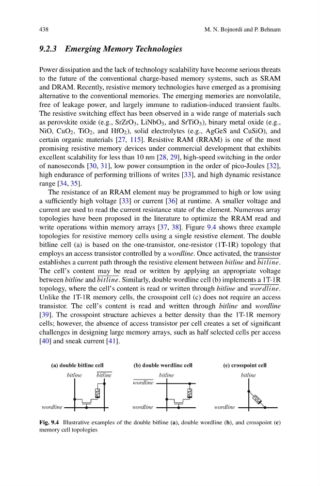
write operations within memory arrays [37, 38]. Figure 9.4 shows three example
topologies for resistive memory cells using a single resistive element. The double
bitline cell (a) is based on the one-transistor, one-resistor (1T-1R) topology that
employs an access transistor controlled by a wordline. Once activated, the transistor
establishes a current path through the resistive element between bitline and bitline.
The cell’s content may be read or written by applying an appropriate voltage
between bitline and bitline. Similarly, double wordline cell (b) implements a 1T-1R
topology, where the cell’s content is read or written through bitline and wordline.
Unlike the 1T-1R memory cells, the crosspoint cell (c) does not require an access
transistor. The cell’s content is read and written through bitline and wordline
[39]. The crosspoint structure achieves a better density than the 1T-1R memory
cells; however, the absence of access transistor per cell creates a set of significant
challenges in designing large memory arrays, such as half selected cells per access
[40] and sneak current [41].
(a) double bitline cell
(b) double wordline cell
wordline
bitline
(c) crosspoint cell
wordline
bitline
bitline
wordline
bitline
wordline
Fig. 9.4 Illustrative examples of the double bitline (a), double wordline (b), and crosspoint (c)
memory cell topologies
M. N. Bojnordi and P. Behnam
9.2.3 Emerging Memory Technologies
Power dissipation and the lack of technology scalability have become serious threats
to the future of the conventional charge-based memory systems, such as SRAM
and DRAM. Recently, resistive memory technologies have emerged as a promising
alternative to the conventional memories. The emerging memories are nonvolatile,
free of leakage power, and largely immune to radiation-induced transient faults.
The resistive switching effect has been observed in a wide range of materials such
as perovskite oxide (e.g., SrZrO 3 , LiNbO 3 , and SrTiO 3 ), binary metal oxide (e.g.,
NiO, CuO 2 , TiO 2 , and HfO 2 ), solid electrolytes (e.g., AgGeS and CuSiO), and
certain organic materials [27, 115]. Resistive RAM (RRAM) is one of the most
promising resistive memory devices under commercial development that exhibits
excellent scalability for less than 10 nm [28, 29], high-speed switching in the order
of nanoseconds [30, 31], low power consumption in the order of pico-Joules [32],
high endurance of performing trillions of writes [33], and high dynamic resistance
range [34, 35].
The resistance of an RRAM element may be programmed to high or low using
a sufficiently high voltage [33] or current [36] at runtime. A smaller voltage and
current are used to read the current resistance state of the element. Numerous array
topologies have been proposed in the literature to optimize the RRAM read and
write operations within memory arrays [37, 38]. Figure 9.4 shows three example
topologies for resistive memory cells using a single resistive element. The double
bitline cell (a) is based on the one-transistor, one-resistor (1T-1R) topology that
employs an access transistor controlled by a wordline. Once activated, the transistor
establishes a current path through the resistive element between bitline and bitline.
The cell’s content may be read or written by applying an appropriate voltage
between bitline and bitline. Similarly, double wordline cell (b) implements a 1T-1R
topology, where the cell’s content is read or written through bitline and wordline.
Unlike the 1T-1R memory cells, the crosspoint cell (c) does not require an access
transistor. The cell’s content is read and written through bitline and wordline
[39]. The crosspoint structure achieves a better density than the 1T-1R memory
cells; however, the absence of access transistor per cell creates a set of significant
challenges in designing large memory arrays, such as half selected cells per access
[40] and sneak current [41].
(a) double bitline cell
(b) double wordline cell
wordline
bitline
(c) crosspoint cell
wordline
bitline
bitline
wordline
bitline
wordline
Fig. 9.4 Illustrative examples of the double bitline (a), double wordline (b), and crosspoint (c)
memory cell topologies