

11 Lithium-Ion Battery—3D Micro-/Nano-Structuring, Modification …
321
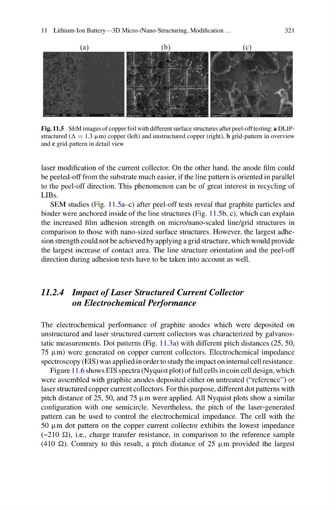
Fig. 11.5 SEM images of copper foil with different surface structures after peel-off testing: a DLIPstructured ( = 1.3 μm) copper (left) and unstructured copper (right), b grid-pattern in overview
and c grid-pattern in detail view
laser modification of the current collector. On the other hand, the anode film could
be peeled-off from the substrate much easier, if the line pattern is oriented in parallel
to the peel-off direction. This phenomenon can be of great interest in recycling of
LIBs.
SEM studies (Fig. 11.5a–c) after peel-off tests reveal that graphite particles and
binder were anchored inside of the line structures (Fig. 11.5b, c), which can explain
the increased film adhesion strength on micro/nano-scaled line/grid structures in
comparison to those with nano-sized surface structures. However, the largest adhesion strength could not be achieved by applying a grid structure, which would provide
the largest increase of contact area. The line structure orientation and the peel-off
direction during adhesion tests have to be taken into account as well.
11.2.4 Impact of Laser Structured Current Collector
on Electrochemical Performance
The electrochemical performance of graphite anodes which were deposited on
unstructured and laser structured current collectors was characterized by galvanostatic measurements. Dot patterns (Fig. 11.3a) with different pitch distances (25, 50,
75 μm) were generated on copper current collectors. Electrochemical impedance
spectroscopy (EIS) was applied in order to study the impact on internal cell resistance.
Figure 11.6 shows EIS spectra (Nyquist plot) of full cells in coin cell design, which
were assembled with graphite anodes deposited either on untreated (“reference”) or
laser structured copper current collectors. For this purpose, different dot patterns with
pitch distance of 25, 50, and 75 μm were applied. All Nyquist plots show a similar
configuration with one semicircle. Nevertheless, the pitch of the laser-generated
pattern can be used to control the electrochemical impedance. The cell with the
50 μm dot pattern on the copper current collector exhibits the lowest impedance
(~210 ), i.e., charge transfer resistance, in comparison to the reference sample
(410 ). Contrary to this result, a pitch distance of 25 μm provided the largest
321
Fig. 11.5 SEM images of copper foil with different surface structures after peel-off testing: a DLIPstructured ( = 1.3 μm) copper (left) and unstructured copper (right), b grid-pattern in overview
and c grid-pattern in detail view
laser modification of the current collector. On the other hand, the anode film could
be peeled-off from the substrate much easier, if the line pattern is oriented in parallel
to the peel-off direction. This phenomenon can be of great interest in recycling of
LIBs.
SEM studies (Fig. 11.5a–c) after peel-off tests reveal that graphite particles and
binder were anchored inside of the line structures (Fig. 11.5b, c), which can explain
the increased film adhesion strength on micro/nano-scaled line/grid structures in
comparison to those with nano-sized surface structures. However, the largest adhesion strength could not be achieved by applying a grid structure, which would provide
the largest increase of contact area. The line structure orientation and the peel-off
direction during adhesion tests have to be taken into account as well.
11.2.4 Impact of Laser Structured Current Collector
on Electrochemical Performance
The electrochemical performance of graphite anodes which were deposited on
unstructured and laser structured current collectors was characterized by galvanostatic measurements. Dot patterns (Fig. 11.3a) with different pitch distances (25, 50,
75 μm) were generated on copper current collectors. Electrochemical impedance
spectroscopy (EIS) was applied in order to study the impact on internal cell resistance.
Figure 11.6 shows EIS spectra (Nyquist plot) of full cells in coin cell design, which
were assembled with graphite anodes deposited either on untreated (“reference”) or
laser structured copper current collectors. For this purpose, different dot patterns with
pitch distance of 25, 50, and 75 μm were applied. All Nyquist plots show a similar
configuration with one semicircle. Nevertheless, the pitch of the laser-generated
pattern can be used to control the electrochemical impedance. The cell with the
50 μm dot pattern on the copper current collector exhibits the lowest impedance
(~210 ), i.e., charge transfer resistance, in comparison to the reference sample
(410 ). Contrary to this result, a pitch distance of 25 μm provided the largest