

3 Apertureless Scanning Near-Field Optical Lithography
129
0
2
4
6
8
1 0
0
1
2
3
4
5
6
Tip- sample distance (nm)
Depth (nm)
0
2
4
6
8
1 0
0
20
40
60
80
100
Tip- sample distance (nm)
Width (nm)
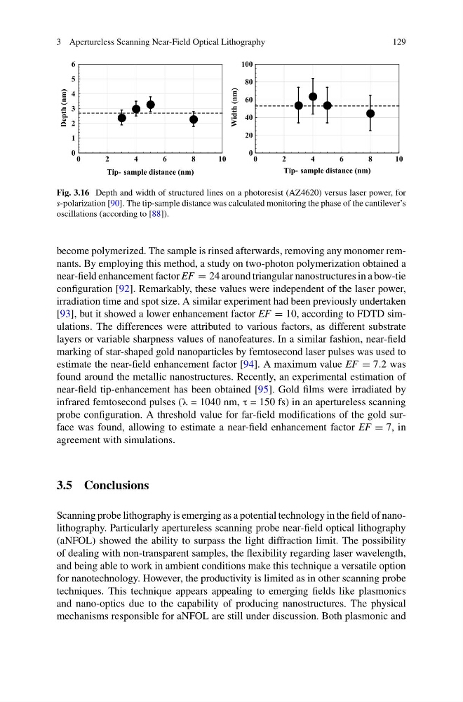
Fig. 3.16 Depth and width of structured lines on a photoresist (AZ4620) versus laser power, for
s-polarization [90]. The tip-sample distance was calculated monitoring the phase of the cantilever’s
oscillations (according to [88]).
become polymerized. The sample is rinsed afterwards, removing any monomer remnants. By employing this method, a study on two-photon polymerization obtained a
near-field enhancement factor EF = 24 around triangular nanostructures in a bow-tie
configuration [92]. Remarkably, these values were independent of the laser power,
irradiation time and spot size. A similar experiment had been previously undertaken
[93], but it showed a lower enhancement factor EF = 10, according to FDTD simulations. The differences were attributed to various factors, as different substrate
layers or variable sharpness values of nanofeatures. In a similar fashion, near-field
marking of star-shaped gold nanoparticles by femtosecond laser pulses was used to
estimate the near-field enhancement factor [94]. A maximum value EF = 7.2 was
found around the metallic nanostructures. Recently, an experimental estimation of
near-field tip-enhancement has been obtained [95]. Gold films were irradiated by
infrared femtosecond pulses (λ = 1040 nm, τ = 150 fs) in an apertureless scanning
probe configuration. A threshold value for far-field modifications of the gold surface was found, allowing to estimate a near-field enhancement factor EF = 7, in
agreement with simulations.
3.5 Conclusions
Scanning probe lithography is emerging as a potential technology in the field of nanolithography. Particularly apertureless scanning probe near-field optical lithography
(aNFOL) showed the ability to surpass the light diffraction limit. The possibility
of dealing with non-transparent samples, the flexibility regarding laser wavelength,
and being able to work in ambient conditions make this technique a versatile option
for nanotechnology. However, the productivity is limited as in other scanning probe
techniques. This technique appears appealing to emerging fields like plasmonics
and nano-optics due to the capability of producing nanostructures. The physical
mechanisms responsible for aNFOL are still under discussion. Both plasmonic and
129
0
2
4
6
8
1 0
0
1
2
3
4
5
6
Tip- sample distance (nm)
Depth (nm)
0
2
4
6
8
1 0
0
20
40
60
80
100
Tip- sample distance (nm)
Width (nm)
Fig. 3.16 Depth and width of structured lines on a photoresist (AZ4620) versus laser power, for
s-polarization [90]. The tip-sample distance was calculated monitoring the phase of the cantilever’s
oscillations (according to [88]).
become polymerized. The sample is rinsed afterwards, removing any monomer remnants. By employing this method, a study on two-photon polymerization obtained a
near-field enhancement factor EF = 24 around triangular nanostructures in a bow-tie
configuration [92]. Remarkably, these values were independent of the laser power,
irradiation time and spot size. A similar experiment had been previously undertaken
[93], but it showed a lower enhancement factor EF = 10, according to FDTD simulations. The differences were attributed to various factors, as different substrate
layers or variable sharpness values of nanofeatures. In a similar fashion, near-field
marking of star-shaped gold nanoparticles by femtosecond laser pulses was used to
estimate the near-field enhancement factor [94]. A maximum value EF = 7.2 was
found around the metallic nanostructures. Recently, an experimental estimation of
near-field tip-enhancement has been obtained [95]. Gold films were irradiated by
infrared femtosecond pulses (λ = 1040 nm, τ = 150 fs) in an apertureless scanning
probe configuration. A threshold value for far-field modifications of the gold surface was found, allowing to estimate a near-field enhancement factor EF = 7, in
agreement with simulations.
3.5 Conclusions
Scanning probe lithography is emerging as a potential technology in the field of nanolithography. Particularly apertureless scanning probe near-field optical lithography
(aNFOL) showed the ability to surpass the light diffraction limit. The possibility
of dealing with non-transparent samples, the flexibility regarding laser wavelength,
and being able to work in ambient conditions make this technique a versatile option
for nanotechnology. However, the productivity is limited as in other scanning probe
techniques. This technique appears appealing to emerging fields like plasmonics
and nano-optics due to the capability of producing nanostructures. The physical
mechanisms responsible for aNFOL are still under discussion. Both plasmonic and