

126
I. Falcón Casas and W. Kautek
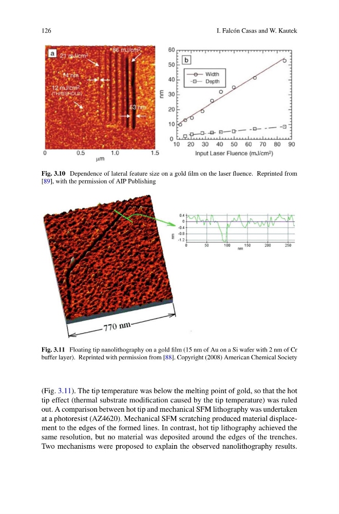
Fig. 3.10 Dependence of lateral feature size on a gold film on the laser fluence. Reprinted from
[89], with the permission of AIP Publishing
Fig. 3.11 Floating tip nanolithography on a gold film (15 nm of Au on a Si wafer with 2 nm of Cr
buffer layer). Reprinted with permission from [88]. Copyright (2008) American Chemical Society
(Fig. 3.11). The tip temperature was below the melting point of gold, so that the hot
tip effect (thermal substrate modification caused by the tip temperature) was ruled
out. A comparison between hot tip and mechanical SFM lithography was undertaken
at a photoresist (AZ4620). Mechanical SFM scratching produced material displacement to the edges of the formed lines. In contrast, hot tip lithography achieved the
same resolution, but no material was deposited around the edges of the trenches.
Two mechanisms were proposed to explain the observed nanolithography results.
I. Falcón Casas and W. Kautek
Fig. 3.10 Dependence of lateral feature size on a gold film on the laser fluence. Reprinted from
[89], with the permission of AIP Publishing
Fig. 3.11 Floating tip nanolithography on a gold film (15 nm of Au on a Si wafer with 2 nm of Cr
buffer layer). Reprinted with permission from [88]. Copyright (2008) American Chemical Society
(Fig. 3.11). The tip temperature was below the melting point of gold, so that the hot
tip effect (thermal substrate modification caused by the tip temperature) was ruled
out. A comparison between hot tip and mechanical SFM lithography was undertaken
at a photoresist (AZ4620). Mechanical SFM scratching produced material displacement to the edges of the formed lines. In contrast, hot tip lithography achieved the
same resolution, but no material was deposited around the edges of the trenches.
Two mechanisms were proposed to explain the observed nanolithography results.