

3 Apertureless Scanning Near-Field Optical Lithography
125
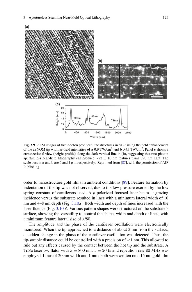
Fig. 3.9 SFM images of two-photon produced line structures in SU-8 using the field enhancement
of the aSNOM tip with far-field intensities of a 0.9 TW/cm 2 and b 0.45 TW/cm 2 . Panel c shows a
crosssectional view (height profile) along the dark vertical line in (b), suggesting that two-photon
apertureless near-field lithography can produce ∼72 ± 10 nm features using 790 nm light. The
scale bars in a and b are 5 and 1 μm respectively. Reprinted from [87], with the permission of AIP
Publishing
order to nanostructure gold films in ambient conditions [89]. Feature formation by
indentation of the tip was not observed, due to the low pressure exerted by the low
spring constant of cantilevers used. A p-polarized focused laser beam at grazing
incidence versus the substrate resulted in lines with a minimum lateral width of 10
nm and 4–8 nm depth (Fig. 3.10a). Both width and depth of lines increased with the
laser fluence (Fig. 3.10b). Various pattern shapes were structured on the substrate’s
surface, showing the versatility to control the shape, width and depth of lines, with
a minimum feature lateral size of λ/80.
The amplitude and the phase of the cantilever oscillation were electronically
monitored. When the tip approached to a distance of about 3 nm from the surface,
a sudden change in the phase of the cantilever oscillation was detected. Thus, the
tip-sample distance could be controlled with a precision of <1 nm. This allowed to
rule out any effects caused by the contact between the hot tip and the substrate. A
Ti:Sa laser oscillator with λ = 800 nm, τ = 20 fs and repetition rate 80 MHz was
employed. Lines of 20 nm width and 1 nm depth were written on a 15 nm gold film
125
Fig. 3.9 SFM images of two-photon produced line structures in SU-8 using the field enhancement
of the aSNOM tip with far-field intensities of a 0.9 TW/cm 2 and b 0.45 TW/cm 2 . Panel c shows a
crosssectional view (height profile) along the dark vertical line in (b), suggesting that two-photon
apertureless near-field lithography can produce ∼72 ± 10 nm features using 790 nm light. The
scale bars in a and b are 5 and 1 μm respectively. Reprinted from [87], with the permission of AIP
Publishing
order to nanostructure gold films in ambient conditions [89]. Feature formation by
indentation of the tip was not observed, due to the low pressure exerted by the low
spring constant of cantilevers used. A p-polarized focused laser beam at grazing
incidence versus the substrate resulted in lines with a minimum lateral width of 10
nm and 4–8 nm depth (Fig. 3.10a). Both width and depth of lines increased with the
laser fluence (Fig. 3.10b). Various pattern shapes were structured on the substrate’s
surface, showing the versatility to control the shape, width and depth of lines, with
a minimum feature lateral size of λ/80.
The amplitude and the phase of the cantilever oscillation were electronically
monitored. When the tip approached to a distance of about 3 nm from the surface,
a sudden change in the phase of the cantilever oscillation was detected. Thus, the
tip-sample distance could be controlled with a precision of <1 nm. This allowed to
rule out any effects caused by the contact between the hot tip and the substrate. A
Ti:Sa laser oscillator with λ = 800 nm, τ = 20 fs and repetition rate 80 MHz was
employed. Lines of 20 nm width and 1 nm depth were written on a 15 nm gold film