

2 Ultrafast Laser Enabling Versatile Fabrication of Surface …
91
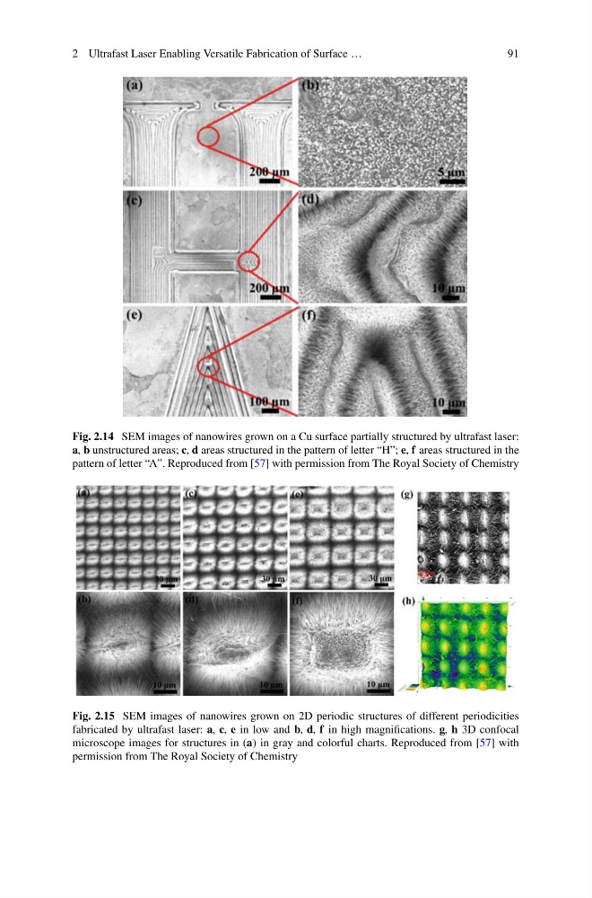
Fig. 2.14 SEM images of nanowires grown on a Cu surface partially structured by ultrafast laser:
a, b unstructured areas; c, d areas structured in the pattern of letter “H”; e, f areas structured in the
pattern of letter “A”. Reproduced from [57] with permission from The Royal Society of Chemistry
Fig. 2.15 SEM images of nanowires grown on 2D periodic structures of different periodicities
fabricated by ultrafast laser: a, c, e in low and b, d, f in high magnifications. g, h 3D confocal
microscope images for structures in (a) in gray and colorful charts. Reproduced from [57] with
permission from The Royal Society of Chemistry
91
Fig. 2.14 SEM images of nanowires grown on a Cu surface partially structured by ultrafast laser:
a, b unstructured areas; c, d areas structured in the pattern of letter “H”; e, f areas structured in the
pattern of letter “A”. Reproduced from [57] with permission from The Royal Society of Chemistry
Fig. 2.15 SEM images of nanowires grown on 2D periodic structures of different periodicities
fabricated by ultrafast laser: a, c, e in low and b, d, f in high magnifications. g, h 3D confocal
microscope images for structures in (a) in gray and colorful charts. Reproduced from [57] with
permission from The Royal Society of Chemistry