

ω
o
ω
C dl
–Z˝
ω
R s
R F
C Ф
0
R s
Z´
R s + R F
125
Fundamentals of Electrochemical Pseudocapacitors
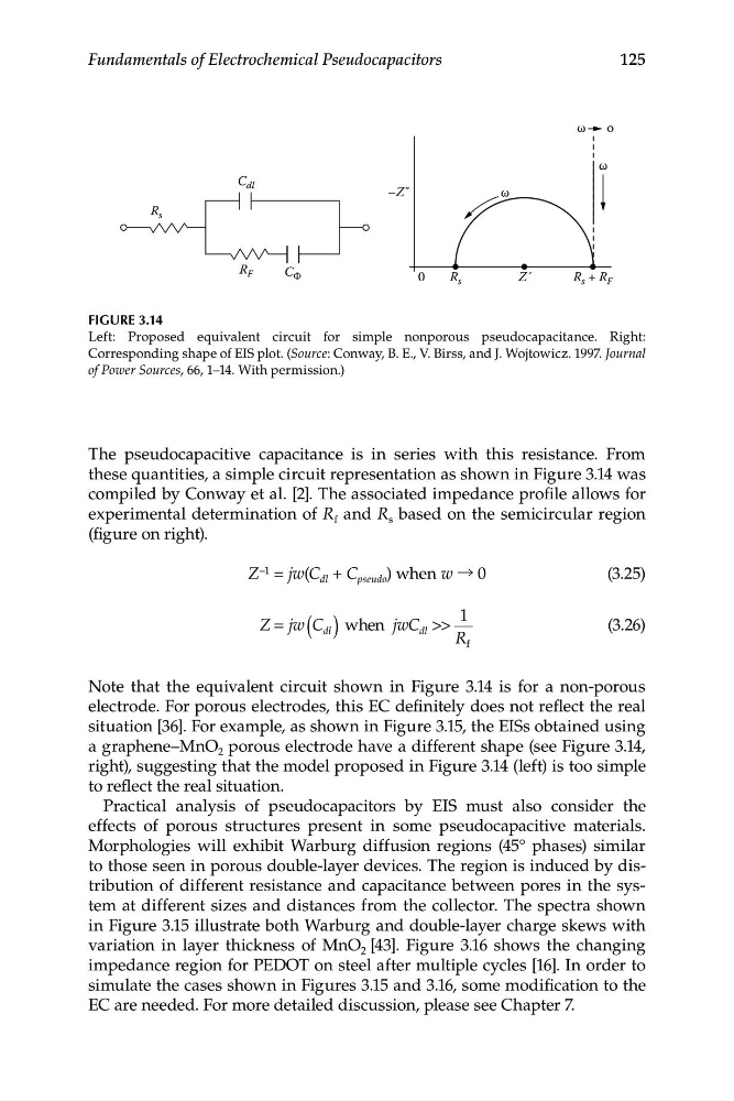
FIGURE 3.14
Left: Proposed equivalent circuit for simple nonporous pseudocapacitance. Right:
Corresponding shape of EIS plot. (Source: Conway, B. E., V. Birss, and J. Wojtowicz. 1997. Journal
of Power Sources, 66, 1–14. With permission.)
The pseudocapacitive capacitance is in series with this resistance. From
these quantities, a simple circuit representation as shown in Figure 3.14 was
compiled by Conway et al. [2]. The associated impedance profile allows for
experimental determination of R f and R s based on the semicircular region
(figure on right).
Z –1 = jw(C dl + C pseudo ) when w → 0
(3.25)
1
Z jw C
( when jwC dl >>
R f
(3.26)
=
dl )
Note that the equivalent circuit shown in Figure 3.14 is for a non-porous
electrode. For porous electrodes, this EC definitely does not reflect the real
situation [36]. For example, as shown in Figure 3.15, the EISs obtained using
a graphene–MnO 2 porous electrode have a different shape (see Figure 3.14,
right), suggesting that the model proposed in Figure 3.14 (left) is too simple
to reflect the real situation.
Practical analysis of pseudocapacitors by EIS must also consider the
effects of porous structures present in some pseudocapacitive materials.
Morphologies will exhibit Warburg diffusion regions (45° phases) similar
to those seen in porous double-layer devices. The region is induced by distribution of different resistance and capacitance between pores in the system at different sizes and distances from the collector. The spectra shown
in Figure 3.15 illustrate both Warburg and double-layer charge skews with
variation in layer thickness of MnO 2 [43]. Figure 3.16 shows the changing
impedance region for PEDOT on steel after multiple cycles [16]. In order to
simulate the cases shown in Figures 3.15 and 3.16, some modification to the
EC are needed. For more detailed discussion, please see Chapter 7.
o
ω
C dl
–Z˝
ω
R s
R F
C Ф
0
R s
Z´
R s + R F
125
Fundamentals of Electrochemical Pseudocapacitors
FIGURE 3.14
Left: Proposed equivalent circuit for simple nonporous pseudocapacitance. Right:
Corresponding shape of EIS plot. (Source: Conway, B. E., V. Birss, and J. Wojtowicz. 1997. Journal
of Power Sources, 66, 1–14. With permission.)
The pseudocapacitive capacitance is in series with this resistance. From
these quantities, a simple circuit representation as shown in Figure 3.14 was
compiled by Conway et al. [2]. The associated impedance profile allows for
experimental determination of R f and R s based on the semicircular region
(figure on right).
Z –1 = jw(C dl + C pseudo ) when w → 0
(3.25)
1
Z jw C
( when jwC dl >>
R f
(3.26)
=
dl )
Note that the equivalent circuit shown in Figure 3.14 is for a non-porous
electrode. For porous electrodes, this EC definitely does not reflect the real
situation [36]. For example, as shown in Figure 3.15, the EISs obtained using
a graphene–MnO 2 porous electrode have a different shape (see Figure 3.14,
right), suggesting that the model proposed in Figure 3.14 (left) is too simple
to reflect the real situation.
Practical analysis of pseudocapacitors by EIS must also consider the
effects of porous structures present in some pseudocapacitive materials.
Morphologies will exhibit Warburg diffusion regions (45° phases) similar
to those seen in porous double-layer devices. The region is induced by distribution of different resistance and capacitance between pores in the system at different sizes and distances from the collector. The spectra shown
in Figure 3.15 illustrate both Warburg and double-layer charge skews with
variation in layer thickness of MnO 2 [43]. Figure 3.16 shows the changing
impedance region for PEDOT on steel after multiple cycles [16]. In order to
simulate the cases shown in Figures 3.15 and 3.16, some modification to the
EC are needed. For more detailed discussion, please see Chapter 7.