

4.6 Epitaxial Technology of High Quality GaN on SiC Substrate
67
of Ceramics of the Chinese Academy of Sciences, Shandong University, Shandong
Tianyue and Hebei Tongguang and other research institutes and enterprises. Mass
production of 3–4 inch SiC substrates has been achieved. The quality and yield of 6
inch SiC substrates are being solved. The research and development of SiC substrates
in China provide convenient conditions for the epitaxial growth of SiC-based GaN
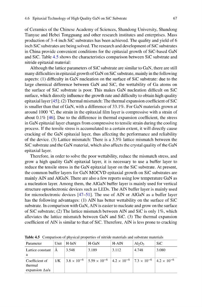
and SiC. Table 4.5 shows the characteristics comparison between SiC substrate and
nitride epitaxial material:
Although the lattice parameters of SiC substrate are similar to GaN, there are still
many difficulties in epitaxial growth of GaN on SiC substrate, mainly in the following
aspects: (1) difficulty in GaN nucleation on the surface of SiC substrate: due to the
large chemical difference between GaN and SiC, the wettability of Ga atoms on
the surface of SiC substrate is poor. This makes GaN nucleation difficult on SiC
surface, which directly influence the growth rate and difficulty to obtain high quality
epitaxial layer [45]; (2) Thermal mismatch: The thermal expansion coefficient of SiC
is smaller than that of GaN, with a difference of 33.1%. For GaN materials grown at
around 1000 °C, the strain in the epitaxial film layer is compressive with a strain of
about 0.1% [46]. Due to the difference in thermal expansion coefficient, the stress
in GaN epitaxial layer changes from compressive to tensile strain during the cooling
process. If the tensile stress is accumulated to a certain extent, it will directly cause
cracking of the GaN epitaxial layer, thus affecting the performance and reliability
of the device. (3) Lattice mismatch: There is a 3.5% lattice mismatch between the
SiC substrate and the GaN material, which also affects the crystal quality of the GaN
epitaxial layer.
Therefore, in order to solve the poor wettability, reduce the mismatch stress, and
grow a high quality GaN epitaxial layer, it is necessary to use a buffer layer to
reduce the tensile stress in the GaN epitaxial layer on the SiC substrate. At present,
the common buffer layers for GaN MOCVD epitaxial growth on SiC substrates are
mainly AlN and AlGaN. There are also a few reports using low temperature GaN as
a nucleation layer. Among them, the AlGaN buffer layer is mainly used for vertical
structure optoelectronic devices such as LEDs. The AlN buffer layer is mainly used
for microelectronic devices [47–51]. The use of AlN or AlGaN as a buffer layer
has the following advantages: (1) AlN has better wettability on the surface of SiC
substrate. In comparison with GaN, AlN is easier to nucleate and grow on the surface
of SiC substrate; (2) The lattice mismatch between AlN and SiC is only 1%, which
alleviates the lattice mismatch between GaN and SiC. (3) The thermal expansion
coefficient of AlN is similar to that of SiC. Therefore, AlN is less prone to cracking
Table 4.5 Comparison of physical properties of nitride materials and substrate materials
Parameter
Unit H-InN
H-GaN
H-AlN
Al 2 O 3
SiC
Lattice constant
a
Å
3.548
3.189
3.112
4.748
3.080
Coefficient of
thermal
expansion a/a
1/K 3.8 × 10 −6 5.59 × 10 −6 4.2 × 10 −6 7.3 × 10 −6 4.2 × 10 −6
67
of Ceramics of the Chinese Academy of Sciences, Shandong University, Shandong
Tianyue and Hebei Tongguang and other research institutes and enterprises. Mass
production of 3–4 inch SiC substrates has been achieved. The quality and yield of 6
inch SiC substrates are being solved. The research and development of SiC substrates
in China provide convenient conditions for the epitaxial growth of SiC-based GaN
and SiC. Table 4.5 shows the characteristics comparison between SiC substrate and
nitride epitaxial material:
Although the lattice parameters of SiC substrate are similar to GaN, there are still
many difficulties in epitaxial growth of GaN on SiC substrate, mainly in the following
aspects: (1) difficulty in GaN nucleation on the surface of SiC substrate: due to the
large chemical difference between GaN and SiC, the wettability of Ga atoms on
the surface of SiC substrate is poor. This makes GaN nucleation difficult on SiC
surface, which directly influence the growth rate and difficulty to obtain high quality
epitaxial layer [45]; (2) Thermal mismatch: The thermal expansion coefficient of SiC
is smaller than that of GaN, with a difference of 33.1%. For GaN materials grown at
around 1000 °C, the strain in the epitaxial film layer is compressive with a strain of
about 0.1% [46]. Due to the difference in thermal expansion coefficient, the stress
in GaN epitaxial layer changes from compressive to tensile strain during the cooling
process. If the tensile stress is accumulated to a certain extent, it will directly cause
cracking of the GaN epitaxial layer, thus affecting the performance and reliability
of the device. (3) Lattice mismatch: There is a 3.5% lattice mismatch between the
SiC substrate and the GaN material, which also affects the crystal quality of the GaN
epitaxial layer.
Therefore, in order to solve the poor wettability, reduce the mismatch stress, and
grow a high quality GaN epitaxial layer, it is necessary to use a buffer layer to
reduce the tensile stress in the GaN epitaxial layer on the SiC substrate. At present,
the common buffer layers for GaN MOCVD epitaxial growth on SiC substrates are
mainly AlN and AlGaN. There are also a few reports using low temperature GaN as
a nucleation layer. Among them, the AlGaN buffer layer is mainly used for vertical
structure optoelectronic devices such as LEDs. The AlN buffer layer is mainly used
for microelectronic devices [47–51]. The use of AlN or AlGaN as a buffer layer
has the following advantages: (1) AlN has better wettability on the surface of SiC
substrate. In comparison with GaN, AlN is easier to nucleate and grow on the surface
of SiC substrate; (2) The lattice mismatch between AlN and SiC is only 1%, which
alleviates the lattice mismatch between GaN and SiC. (3) The thermal expansion
coefficient of AlN is similar to that of SiC. Therefore, AlN is less prone to cracking
Table 4.5 Comparison of physical properties of nitride materials and substrate materials
Parameter
Unit H-InN
H-GaN
H-AlN
Al 2 O 3
SiC
Lattice constant
a
Å
3.548
3.189
3.112
4.748
3.080
Coefficient of
thermal
expansion a/a
1/K 3.8 × 10 −6 5.59 × 10 −6 4.2 × 10 −6 7.3 × 10 −6 4.2 × 10 −6