

56
4 Epitaxial of III-Nitride LED Materials
4.5.1.2 Effect of the Growth Temperature of Buffer Layer
It can be seen from Table 4.3 that different temperature to grow buffer layer has a
great influence on the electrical properties of the material. As the growth temperature
of the buffer layer increases (515–535 °C), the carrier mobility of the intrinsic GaN
material increases significantly, and the background carrier concentration decreases.
Nevertheless, higher temperature (550 °C, data is not listed) to grow buffer layer can
result in a decreased carrier mobility. It indicates that a suitable growth temperature
for buffer layer can improve the crystal quality of the intrinsic GaN material.
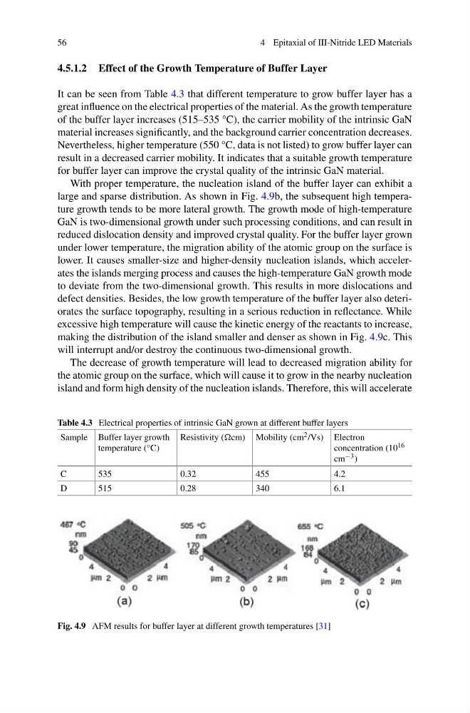
With proper temperature, the nucleation island of the buffer layer can exhibit a
large and sparse distribution. As shown in Fig. 4.9b, the subsequent high temperature growth tends to be more lateral growth. The growth mode of high-temperature
GaN is two-dimensional growth under such processing conditions, and can result in
reduced dislocation density and improved crystal quality. For the buffer layer grown
under lower temperature, the migration ability of the atomic group on the surface is
lower. It causes smaller-size and higher-density nucleation islands, which accelerates the islands merging process and causes the high-temperature GaN growth mode
to deviate from the two-dimensional growth. This results in more dislocations and
defect densities. Besides, the low growth temperature of the buffer layer also deteriorates the surface topography, resulting in a serious reduction in reflectance. While
excessive high temperature will cause the kinetic energy of the reactants to increase,
making the distribution of the island smaller and denser as shown in Fig. 4.9c. This
will interrupt and/or destroy the continuous two-dimensional growth.
The decrease of growth temperature will lead to decreased migration ability for
the atomic group on the surface, which will cause it to grow in the nearby nucleation
island and form high density of the nucleation islands. Therefore, this will accelerate
Table 4.3 Electrical properties of intrinsic GaN grown at different buffer layers
Sample Buffer layer growth
temperature (°C)
Resistivity (cm) Mobility (cm 2 /Vs) Electron
concentration (10 16
cm −3 )
C
535
0.32
455
4.2
D
515
0.28
340
6.1
Fig. 4.9 AFM results for buffer layer at different growth temperatures [31]
4 Epitaxial of III-Nitride LED Materials
4.5.1.2 Effect of the Growth Temperature of Buffer Layer
It can be seen from Table 4.3 that different temperature to grow buffer layer has a
great influence on the electrical properties of the material. As the growth temperature
of the buffer layer increases (515–535 °C), the carrier mobility of the intrinsic GaN
material increases significantly, and the background carrier concentration decreases.
Nevertheless, higher temperature (550 °C, data is not listed) to grow buffer layer can
result in a decreased carrier mobility. It indicates that a suitable growth temperature
for buffer layer can improve the crystal quality of the intrinsic GaN material.
With proper temperature, the nucleation island of the buffer layer can exhibit a
large and sparse distribution. As shown in Fig. 4.9b, the subsequent high temperature growth tends to be more lateral growth. The growth mode of high-temperature
GaN is two-dimensional growth under such processing conditions, and can result in
reduced dislocation density and improved crystal quality. For the buffer layer grown
under lower temperature, the migration ability of the atomic group on the surface is
lower. It causes smaller-size and higher-density nucleation islands, which accelerates the islands merging process and causes the high-temperature GaN growth mode
to deviate from the two-dimensional growth. This results in more dislocations and
defect densities. Besides, the low growth temperature of the buffer layer also deteriorates the surface topography, resulting in a serious reduction in reflectance. While
excessive high temperature will cause the kinetic energy of the reactants to increase,
making the distribution of the island smaller and denser as shown in Fig. 4.9c. This
will interrupt and/or destroy the continuous two-dimensional growth.
The decrease of growth temperature will lead to decreased migration ability for
the atomic group on the surface, which will cause it to grow in the nearby nucleation
island and form high density of the nucleation islands. Therefore, this will accelerate
Table 4.3 Electrical properties of intrinsic GaN grown at different buffer layers
Sample Buffer layer growth
temperature (°C)
Resistivity (cm) Mobility (cm 2 /Vs) Electron
concentration (10 16
cm −3 )
C
535
0.32
455
4.2
D
515
0.28
340
6.1
Fig. 4.9 AFM results for buffer layer at different growth temperatures [31]