

4.5 Influence of Growth Conditions on Epitaxial Layer Quality …
55
mobility decreases as the thickness of the buffer layer decreases. This is consistent
with the XRD results, which also indicates the epitaxial material with thin buffer
layer has poor crystal quality. Poor quality of high temperature epitaxial layer by
using thin buffer layer can be attributed to a loose distribution of nucleation islands
that are not favorable seed crystals for the lateral growth. In other words, they cannot
provide a good template for the growth of the subsequent high temperature GaN
film, making the high-temperature growth mode away from the two-dimensional
growth and therefore a high dislocation density and poor crystal quality [26–28].
According to the results of Kuznia et al. [29], the optimized buffer layer thickness
should be between 20 and 30 nm. Further increasing the thickness of the buffer layer
also causes the deterioration of crystal quality. Therefore, much thicker buffer layer
is not widely investigated.
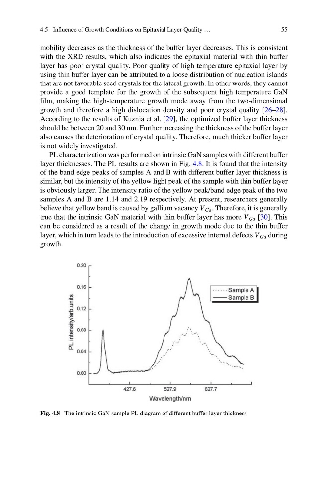
PL characterization was performed on intrinsic GaN samples with different buffer
layer thicknesses. The PL results are shown in Fig. 4.8. It is found that the intensity
of the band edge peaks of samples A and B with different buffer layer thickness is
similar, but the intensity of the yellow light peak of the sample with thin buffer layer
is obviously larger. The intensity ratio of the yellow peak/band edge peak of the two
samples A and B are 1.14 and 2.19 respectively. At present, researchers generally
believe that yellow band is caused by gallium vacancy V Ga . Therefore, it is generally
true that the intrinsic GaN material with thin buffer layer has more V Ga [30]. This
can be considered as a result of the change in growth mode due to the thin buffer
layer, which in turn leads to the introduction of excessive internal defects V Ga during
growth.
Fig. 4.8 The intrinsic GaN sample PL diagram of different buffer layer thickness
55
mobility decreases as the thickness of the buffer layer decreases. This is consistent
with the XRD results, which also indicates the epitaxial material with thin buffer
layer has poor crystal quality. Poor quality of high temperature epitaxial layer by
using thin buffer layer can be attributed to a loose distribution of nucleation islands
that are not favorable seed crystals for the lateral growth. In other words, they cannot
provide a good template for the growth of the subsequent high temperature GaN
film, making the high-temperature growth mode away from the two-dimensional
growth and therefore a high dislocation density and poor crystal quality [26–28].
According to the results of Kuznia et al. [29], the optimized buffer layer thickness
should be between 20 and 30 nm. Further increasing the thickness of the buffer layer
also causes the deterioration of crystal quality. Therefore, much thicker buffer layer
is not widely investigated.
PL characterization was performed on intrinsic GaN samples with different buffer
layer thicknesses. The PL results are shown in Fig. 4.8. It is found that the intensity
of the band edge peaks of samples A and B with different buffer layer thickness is
similar, but the intensity of the yellow light peak of the sample with thin buffer layer
is obviously larger. The intensity ratio of the yellow peak/band edge peak of the two
samples A and B are 1.14 and 2.19 respectively. At present, researchers generally
believe that yellow band is caused by gallium vacancy V Ga . Therefore, it is generally
true that the intrinsic GaN material with thin buffer layer has more V Ga [30]. This
can be considered as a result of the change in growth mode due to the thin buffer
layer, which in turn leads to the introduction of excessive internal defects V Ga during
growth.
Fig. 4.8 The intrinsic GaN sample PL diagram of different buffer layer thickness