

22
3 Properties and Testing of Group III-Nitride LED Materials
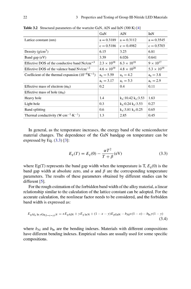
Table 3.2 Structural parameters of the wurtzite GaN, AlN and InN (300 K) [4]
GaN
AlN
InN
Lattice constant (nm)
a = 0.3189 a = 0.3112
a = 0.3545
c = 0.5186 c = 0.4982
c = 0.5703
Density (g/cm 3 )
6.15
3.23
6.81
Band gap (eV)
3.39
6.026
0.641
Effective DOS of the conductive band Nc/cm −3 2.3 × 10 18 6.3 × 10 18
9 × 10 17
Effective DOS of the valence band Nv/cm −3
4.6 × 10 19 4.8 × 10 20
5.3 × 10 19
Coefficient of the thermal expansion (10 −6 K −1 ) a a = 5.59
a a = 4.2
a a = 3.8
a c = 3.17
a c = 5.3
a c = 2.9
Effective mass of electron (m 0 )
0.2
0.4
0.11
Effective mass of hole (m 0 )
Heavy hole
1.4
k x :10.42 k z :3.53 1.63
Light hole
0.3
k x :0.24 k z :3.53
0.27
Band splitting
0.6
k x :3.81 k z :0.25
0.65
Thermal conductivity (W·cm −1 ·K −1 )
1.3
2.85
0.45
In general, as the temperature increases, the energy band of the semiconductor
material changes. The dependence of the GaN bandgap on temperature can be
expressed by Eq. (3.3) [3]:
E g (T ) = E g (0) −
αT
2
T + β
(eV)
(3.3)
where Eg(T) represents the band gap width when the temperature is T, E g (0) is the
band gap width at absolute zero, and α and β are the corresponding temperature
parameters. The results of these parameters obtained by different studies can be
different [5].
For the rough estimation of the forbidden band width of the alloy material, a linear
relationship similar to the calculation of the lattice constant can be adopted. For the
accurate calculation, the nonlinear factor needs to be considered, and the forbidden
band width is expressed as:
E gAl x ln yGa (1−x−y) N = x E gAlN + y E g ln N + (1 − x − y)E gGaN − b Al x(1 − x) − b ln y(1 − y)
(3.4)
where b Al and b In are the bending indexes. Materials with different compositions
have different bending indexes. Empirical values are usually used for some specific
compositions.
3 Properties and Testing of Group III-Nitride LED Materials
Table 3.2 Structural parameters of the wurtzite GaN, AlN and InN (300 K) [4]
GaN
AlN
InN
Lattice constant (nm)
a = 0.3189 a = 0.3112
a = 0.3545
c = 0.5186 c = 0.4982
c = 0.5703
Density (g/cm 3 )
6.15
3.23
6.81
Band gap (eV)
3.39
6.026
0.641
Effective DOS of the conductive band Nc/cm −3 2.3 × 10 18 6.3 × 10 18
9 × 10 17
Effective DOS of the valence band Nv/cm −3
4.6 × 10 19 4.8 × 10 20
5.3 × 10 19
Coefficient of the thermal expansion (10 −6 K −1 ) a a = 5.59
a a = 4.2
a a = 3.8
a c = 3.17
a c = 5.3
a c = 2.9
Effective mass of electron (m 0 )
0.2
0.4
0.11
Effective mass of hole (m 0 )
Heavy hole
1.4
k x :10.42 k z :3.53 1.63
Light hole
0.3
k x :0.24 k z :3.53
0.27
Band splitting
0.6
k x :3.81 k z :0.25
0.65
Thermal conductivity (W·cm −1 ·K −1 )
1.3
2.85
0.45
In general, as the temperature increases, the energy band of the semiconductor
material changes. The dependence of the GaN bandgap on temperature can be
expressed by Eq. (3.3) [3]:
E g (T ) = E g (0) −
αT
2
T + β
(eV)
(3.3)
where Eg(T) represents the band gap width when the temperature is T, E g (0) is the
band gap width at absolute zero, and α and β are the corresponding temperature
parameters. The results of these parameters obtained by different studies can be
different [5].
For the rough estimation of the forbidden band width of the alloy material, a linear
relationship similar to the calculation of the lattice constant can be adopted. For the
accurate calculation, the nonlinear factor needs to be considered, and the forbidden
band width is expressed as:
E gAl x ln yGa (1−x−y) N = x E gAlN + y E g ln N + (1 − x − y)E gGaN − b Al x(1 − x) − b ln y(1 − y)
(3.4)
where b Al and b In are the bending indexes. Materials with different compositions
have different bending indexes. Empirical values are usually used for some specific
compositions.