

3.1 Crystal Structure and Band Structure of Group III Nitride
21
a Al x I n y Ga 1−x−y N = x × a Al N + y × a I nN + (1 − x − y) × a Ga N
(3.1)
c Al x I n y Ga 1−x−y N = x × c Al N + y × c I nN + (1 − x − y) × c I nN
(3.2)
wherein a Al N , c Al N , a I nN , c I nN , a Ga N , c I nN represent lattice constants of the AlN,
InN, and GaN binary compounds, respectively.
3.1.2 Band Structure
In the energy band theory, the problem can be described and analyzed more clearly
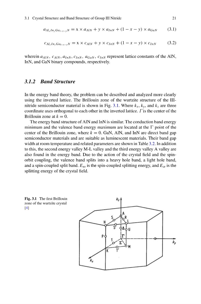
using the inverted lattice. The Brillouin zone of the wurtzite structure of the IIInitride semiconductor material is shown in Fig. 3.1. Where k x , k y , and k z are three
coordinate axes orthogonal to each other in the inverted lattice. G is the center of the
Brillouin zone at k = 0.
The energy band structure of AlN and InN is similar. The conduction band energy
minimum and the valence band energy maximum are located at the G point of the
center of the Brillouin zone, where k = 0. GaN, AlN, and InN are direct band gap
semiconductor materials and are suitable as luminescent materials. Their band gap
width at room temperature and related parameters are shown in Table 3.2. In addition
to this, the second energy valley M-L valley and the third energy valley A valley are
also found in the energy band. Due to the action of the crystal field and the spinorbit coupling, the valence band splits into a heavy hole band, a light hole band,
and a spin-coupled split band. E so is the spin-coupled splitting energy, and E cr is the
splitting energy of the crystal field.
Fig. 3.1 The first Brillouin
zone of the wurtzite crystal
[4]
21
a Al x I n y Ga 1−x−y N = x × a Al N + y × a I nN + (1 − x − y) × a Ga N
(3.1)
c Al x I n y Ga 1−x−y N = x × c Al N + y × c I nN + (1 − x − y) × c I nN
(3.2)
wherein a Al N , c Al N , a I nN , c I nN , a Ga N , c I nN represent lattice constants of the AlN,
InN, and GaN binary compounds, respectively.
3.1.2 Band Structure
In the energy band theory, the problem can be described and analyzed more clearly
using the inverted lattice. The Brillouin zone of the wurtzite structure of the IIInitride semiconductor material is shown in Fig. 3.1. Where k x , k y , and k z are three
coordinate axes orthogonal to each other in the inverted lattice. G is the center of the
Brillouin zone at k = 0.
The energy band structure of AlN and InN is similar. The conduction band energy
minimum and the valence band energy maximum are located at the G point of the
center of the Brillouin zone, where k = 0. GaN, AlN, and InN are direct band gap
semiconductor materials and are suitable as luminescent materials. Their band gap
width at room temperature and related parameters are shown in Table 3.2. In addition
to this, the second energy valley M-L valley and the third energy valley A valley are
also found in the energy band. Due to the action of the crystal field and the spinorbit coupling, the valence band splits into a heavy hole band, a light hole band,
and a spin-coupled split band. E so is the spin-coupled splitting energy, and E cr is the
splitting energy of the crystal field.
Fig. 3.1 The first Brillouin
zone of the wurtzite crystal
[4]