

262
12 Novel Nitride LED Technology
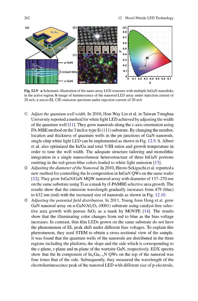
Fig. 12.9 a Schematic illustration of the nano-array LED structure with multiple InGaN nanodisks
in the active region; b image of luminescence of the nanorod LED array under injection current of
20 mA; c micro-EL CIE emission spectrum under injection current of 20 mA
➀ Adjust the quantum well width. In 2010, Hon-Way Lin et al. in Taiwan Tsinghua
University reported a method for white light LED achieved by adjusting the width
of the quantum well [11]. They grow nanorods along the c-axis orientation using
PA-MBE method on the 3 inch n-type Si (111) substrate. By changing the number,
location and thickness of quantum wells in the pn junctions of GaN nanorods,
single-chip white light LED can be implemented as shown in Fig. 12.9. S. Albert
et al. also optimized the In/Ga and total V/III ratios and growth temperature in
order to tune the well width. The adequate structure tailoring and monolithic
integration in a single nanocolumnar heterostructure of three InGaN portions
emitting in the red-green-blue colors leaded to white light emission [13].
➁ Adjusting the diameter of the Nanorod. In 2010, Hiroto Sekiguchi et al. reported a
new method for controlling the In composition in InGaN QWs on the same wafer
[12]. They grow InGaN/GaN MQW nanorod array with diameter of 137–270 nm
on the same substrate using Ti as a mask by rf-PAMBE selective area growth. The
results show that the emission wavelength gradually increases from 479 (blue)
to 632 nm (red) with the increased size of nanorods as shown in Fig. 12.10.
➂ Adjusting the potential field distribution. In 2011, Young Joon Hong et al. grew
GaN nanorod array on n-GaN/Al 2 O 3 (0001) substrate using catalyst-free selective area growth with porous SiO 2 as a mask by MOVPE [14]. The results
show that the illuminating color changes from red to blue as the bias voltage
increases. In contrast, thin film LEDs grown on the same substrate do not have
the phenomenon of EL peak shift under different bias voltages. To explain this
phenomenon, they used STEM to obtain a cross-sectional view of the sample.
It was found that the quantum wells of the nanorods are distributed in the three
regions including the platform, the slope and the side which is corresponding to
the c-plane, r-plane and m-plane of the wurtzite GaN, respectively. EDX spectra
show that the In component of In x Ga 1–x N QWs on the top of the nanorod was
four times that of the side. Subsequently, they measured the wavelength of the
electroluminescence peak of the nanorod LED with different size of p-electrode,
12 Novel Nitride LED Technology
Fig. 12.9 a Schematic illustration of the nano-array LED structure with multiple InGaN nanodisks
in the active region; b image of luminescence of the nanorod LED array under injection current of
20 mA; c micro-EL CIE emission spectrum under injection current of 20 mA
➀ Adjust the quantum well width. In 2010, Hon-Way Lin et al. in Taiwan Tsinghua
University reported a method for white light LED achieved by adjusting the width
of the quantum well [11]. They grow nanorods along the c-axis orientation using
PA-MBE method on the 3 inch n-type Si (111) substrate. By changing the number,
location and thickness of quantum wells in the pn junctions of GaN nanorods,
single-chip white light LED can be implemented as shown in Fig. 12.9. S. Albert
et al. also optimized the In/Ga and total V/III ratios and growth temperature in
order to tune the well width. The adequate structure tailoring and monolithic
integration in a single nanocolumnar heterostructure of three InGaN portions
emitting in the red-green-blue colors leaded to white light emission [13].
➁ Adjusting the diameter of the Nanorod. In 2010, Hiroto Sekiguchi et al. reported a
new method for controlling the In composition in InGaN QWs on the same wafer
[12]. They grow InGaN/GaN MQW nanorod array with diameter of 137–270 nm
on the same substrate using Ti as a mask by rf-PAMBE selective area growth. The
results show that the emission wavelength gradually increases from 479 (blue)
to 632 nm (red) with the increased size of nanorods as shown in Fig. 12.10.
➂ Adjusting the potential field distribution. In 2011, Young Joon Hong et al. grew
GaN nanorod array on n-GaN/Al 2 O 3 (0001) substrate using catalyst-free selective area growth with porous SiO 2 as a mask by MOVPE [14]. The results
show that the illuminating color changes from red to blue as the bias voltage
increases. In contrast, thin film LEDs grown on the same substrate do not have
the phenomenon of EL peak shift under different bias voltages. To explain this
phenomenon, they used STEM to obtain a cross-sectional view of the sample.
It was found that the quantum wells of the nanorods are distributed in the three
regions including the platform, the slope and the side which is corresponding to
the c-plane, r-plane and m-plane of the wurtzite GaN, respectively. EDX spectra
show that the In component of In x Ga 1–x N QWs on the top of the nanorod was
four times that of the side. Subsequently, they measured the wavelength of the
electroluminescence peak of the nanorod LED with different size of p-electrode,