

12.1 GaN-Based Nanorod LED
263
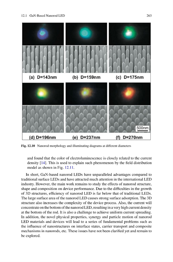
Fig. 12.10 Nanorod morphology and illuminating diagrams at different diameters
and found that the color of electroluminescence is closely related to the current
density [14]. This is used to explain such phenomenon by the field distribution
model as shown in Fig. 12.11.
In short, GaN-based nanorod LEDs have unparalleled advantages compared to
traditional surface LEDs and have attracted much attention in the international LED
industry. However, the main work remains to study the effects of nanorod structure,
shape and composition on device performance. Due to the difficulties in the growth
of 3D structures, efficiency of nanorod LED is far below that of traditional LEDs.
The large surface area of the nanorod LED causes strong surface adsorption. The 3D
structure also increases the complexity of the device process. Also, the current will
concentrate on the bottom of the nanorod LED, resulting in a very high current density
at the bottom of the rod. It is also a challenge to achieve uniform current spreading.
In addition, the novel physical properties, synergy and particle motion of nanorod
LED materials and devices will lead to a series of fundamental problems such as
the influence of nanostructures on interface states, carrier transport and composite
mechanisms in nanorods, etc. These issues have not been clarified yet and remain to
be explored.
263
Fig. 12.10 Nanorod morphology and illuminating diagrams at different diameters
and found that the color of electroluminescence is closely related to the current
density [14]. This is used to explain such phenomenon by the field distribution
model as shown in Fig. 12.11.
In short, GaN-based nanorod LEDs have unparalleled advantages compared to
traditional surface LEDs and have attracted much attention in the international LED
industry. However, the main work remains to study the effects of nanorod structure,
shape and composition on device performance. Due to the difficulties in the growth
of 3D structures, efficiency of nanorod LED is far below that of traditional LEDs.
The large surface area of the nanorod LED causes strong surface adsorption. The 3D
structure also increases the complexity of the device process. Also, the current will
concentrate on the bottom of the nanorod LED, resulting in a very high current density
at the bottom of the rod. It is also a challenge to achieve uniform current spreading.
In addition, the novel physical properties, synergy and particle motion of nanorod
LED materials and devices will lead to a series of fundamental problems such as
the influence of nanostructures on interface states, carrier transport and composite
mechanisms in nanorods, etc. These issues have not been clarified yet and remain to
be explored.