

140
7 III-Nitride LED Quantum Efficiency Improvement Technology
7.4.3 Current Blocking Technique
There are many discussions about reasons of efficiency droop resulted from Auger
recombination [30] and leakage of carriers [31, 32]. In localization in the quantum
well is also considered [33]. But there is no mention of the efficiency droop caused
by current distribution. From the previous calculation and analysis of the current
distribution, it can be seen that the current distribution under the larger current is
more uneven. The light absorption from the metal electrode can be large. All of these
can lead to LED efficiency droop. The reason for the current fluctuation of the current
injected into the multiple quantum wells in the chip changing with the increase of
the injection current is that the PN junction dynamic resistance of the LED is not a
fixed value which decreases with the increase of the current density. Therefore, the
current spreading length in the current spreading layer of the LED is different under
different injection currents which have been analyzed in the prior art.
On the other hand, the current density injected into different regions of the multiple
quantum wells is different in practical LED devices. Different injection current densities will form different carrier concentrations in the quantum wells. In other words,
the internal quantum efficiency is not the same at deferent carrier concentrations.
Therefore, there are different internal quantum efficiencies in different regions of
the chip. This also indicates that the overall efficiency of the device is related to the
distribution of current density [34].
The function of the current blocking layer is to limit the injection current under
the n electrode, where the light generated by this partially injected current is difficult
to extract. Mathematically, the value of the second term of the denominator in the
above formula is reduced to zero, thereby reducing the denominator and increasing
the value of the fraction.
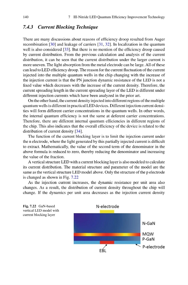
A vertical structure LED with a current blocking layer is also modeled to calculate
its current distribution. The material structure and parameter of the model are the
same as the vertical structure LED model above. Only the structure of the p electrode
is changed as shown in Fig. 7.22
As the injection current increases, the dynamic resistance per unit area also
changes. As a result, the distribution of current density throughout the chip will
change. If the dynamics per unit area decreases as the injection current density
Fig. 7.22 GaN-based
vertical LED model with
current blocking layer
7 III-Nitride LED Quantum Efficiency Improvement Technology
7.4.3 Current Blocking Technique
There are many discussions about reasons of efficiency droop resulted from Auger
recombination [30] and leakage of carriers [31, 32]. In localization in the quantum
well is also considered [33]. But there is no mention of the efficiency droop caused
by current distribution. From the previous calculation and analysis of the current
distribution, it can be seen that the current distribution under the larger current is
more uneven. The light absorption from the metal electrode can be large. All of these
can lead to LED efficiency droop. The reason for the current fluctuation of the current
injected into the multiple quantum wells in the chip changing with the increase of
the injection current is that the PN junction dynamic resistance of the LED is not a
fixed value which decreases with the increase of the current density. Therefore, the
current spreading length in the current spreading layer of the LED is different under
different injection currents which have been analyzed in the prior art.
On the other hand, the current density injected into different regions of the multiple
quantum wells is different in practical LED devices. Different injection current densities will form different carrier concentrations in the quantum wells. In other words,
the internal quantum efficiency is not the same at deferent carrier concentrations.
Therefore, there are different internal quantum efficiencies in different regions of
the chip. This also indicates that the overall efficiency of the device is related to the
distribution of current density [34].
The function of the current blocking layer is to limit the injection current under
the n electrode, where the light generated by this partially injected current is difficult
to extract. Mathematically, the value of the second term of the denominator in the
above formula is reduced to zero, thereby reducing the denominator and increasing
the value of the fraction.
A vertical structure LED with a current blocking layer is also modeled to calculate
its current distribution. The material structure and parameter of the model are the
same as the vertical structure LED model above. Only the structure of the p electrode
is changed as shown in Fig. 7.22
As the injection current increases, the dynamic resistance per unit area also
changes. As a result, the distribution of current density throughout the chip will
change. If the dynamics per unit area decreases as the injection current density
Fig. 7.22 GaN-based
vertical LED model with
current blocking layer