

138
7 III-Nitride LED Quantum Efficiency Improvement Technology
J x = q · μ · n ·
dV (x)
dx
(7.13)
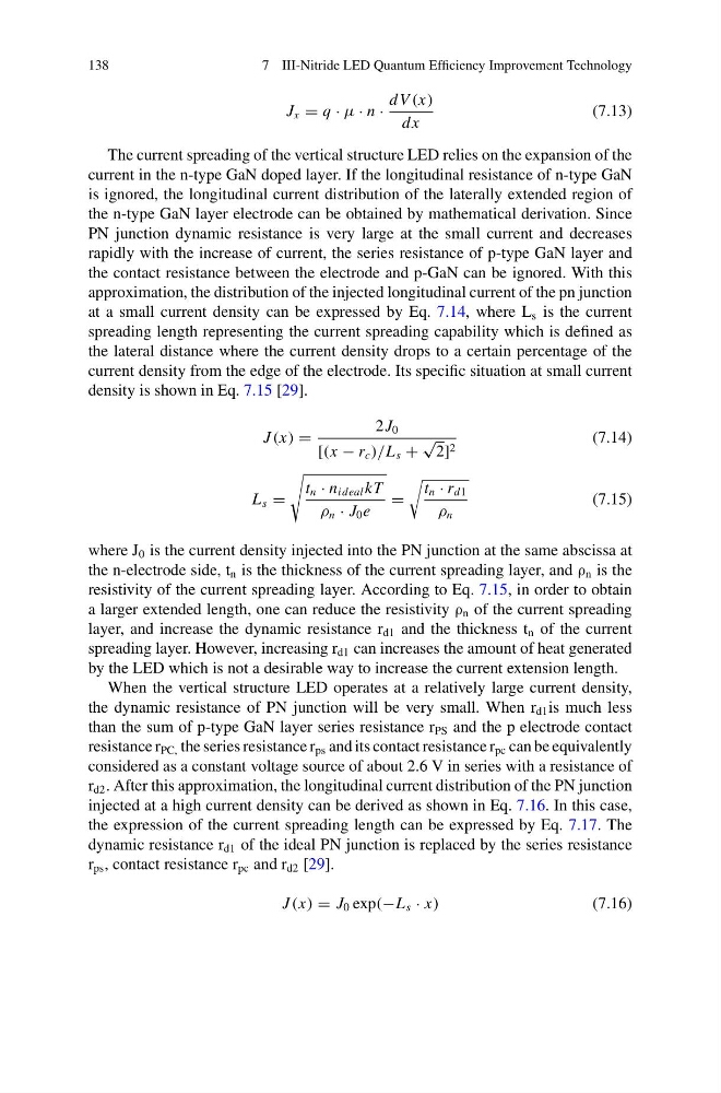
The current spreading of the vertical structure LED relies on the expansion of the
current in the n-type GaN doped layer. If the longitudinal resistance of n-type GaN
is ignored, the longitudinal current distribution of the laterally extended region of
the n-type GaN layer electrode can be obtained by mathematical derivation. Since
PN junction dynamic resistance is very large at the small current and decreases
rapidly with the increase of current, the series resistance of p-type GaN layer and
the contact resistance between the electrode and p-GaN can be ignored. With this
approximation, the distribution of the injected longitudinal current of the pn junction
at a small current density can be expressed by Eq. 7.14, where L s is the current
spreading length representing the current spreading capability which is defined as
the lateral distance where the current density drops to a certain percentage of the
current density from the edge of the electrode. Its specific situation at small current
density is shown in Eq. 7.15 [29].
J (x) =
2J 0
[(x − r c )/L s +
√
2] 2
(7.14)
L s =
t n · n ideal kT
ρ n · J 0 e
=
t n · r d1
ρ n
(7.15)
where J 0 is the current density injected into the PN junction at the same abscissa at
the n-electrode side, t n is the thickness of the current spreading layer, and ρ n is the
resistivity of the current spreading layer. According to Eq. 7.15, in order to obtain
a larger extended length, one can reduce the resistivity ρ n of the current spreading
layer, and increase the dynamic resistance r d1 and the thickness t n of the current
spreading layer. However, increasing r d1 can increases the amount of heat generated
by the LED which is not a desirable way to increase the current extension length.
When the vertical structure LED operates at a relatively large current density,
the dynamic resistance of PN junction will be very small. When r d1 is much less
than the sum of p-type GaN layer series resistance r PS and the p electrode contact
resistance r PC, the series resistance r ps and its contact resistance r pc can be equivalently
considered as a constant voltage source of about 2.6 V in series with a resistance of
r d2 . After this approximation, the longitudinal current distribution of the PN junction
injected at a high current density can be derived as shown in Eq. 7.16. In this case,
the expression of the current spreading length can be expressed by Eq. 7.17. The
dynamic resistance r d1 of the ideal PN junction is replaced by the series resistance
r ps , contact resistance r pc and r d2 [29].
J (x) = J 0 exp(−L s · x)
(7.16)
7 III-Nitride LED Quantum Efficiency Improvement Technology
J x = q · μ · n ·
dV (x)
dx
(7.13)
The current spreading of the vertical structure LED relies on the expansion of the
current in the n-type GaN doped layer. If the longitudinal resistance of n-type GaN
is ignored, the longitudinal current distribution of the laterally extended region of
the n-type GaN layer electrode can be obtained by mathematical derivation. Since
PN junction dynamic resistance is very large at the small current and decreases
rapidly with the increase of current, the series resistance of p-type GaN layer and
the contact resistance between the electrode and p-GaN can be ignored. With this
approximation, the distribution of the injected longitudinal current of the pn junction
at a small current density can be expressed by Eq. 7.14, where L s is the current
spreading length representing the current spreading capability which is defined as
the lateral distance where the current density drops to a certain percentage of the
current density from the edge of the electrode. Its specific situation at small current
density is shown in Eq. 7.15 [29].
J (x) =
2J 0
[(x − r c )/L s +
√
2] 2
(7.14)
L s =
t n · n ideal kT
ρ n · J 0 e
=
t n · r d1
ρ n
(7.15)
where J 0 is the current density injected into the PN junction at the same abscissa at
the n-electrode side, t n is the thickness of the current spreading layer, and ρ n is the
resistivity of the current spreading layer. According to Eq. 7.15, in order to obtain
a larger extended length, one can reduce the resistivity ρ n of the current spreading
layer, and increase the dynamic resistance r d1 and the thickness t n of the current
spreading layer. However, increasing r d1 can increases the amount of heat generated
by the LED which is not a desirable way to increase the current extension length.
When the vertical structure LED operates at a relatively large current density,
the dynamic resistance of PN junction will be very small. When r d1 is much less
than the sum of p-type GaN layer series resistance r PS and the p electrode contact
resistance r PC, the series resistance r ps and its contact resistance r pc can be equivalently
considered as a constant voltage source of about 2.6 V in series with a resistance of
r d2 . After this approximation, the longitudinal current distribution of the PN junction
injected at a high current density can be derived as shown in Eq. 7.16. In this case,
the expression of the current spreading length can be expressed by Eq. 7.17. The
dynamic resistance r d1 of the ideal PN junction is replaced by the series resistance
r ps , contact resistance r pc and r d2 [29].
J (x) = J 0 exp(−L s · x)
(7.16)