

7.4 Current Injection Efficiency Improvement Technology
137
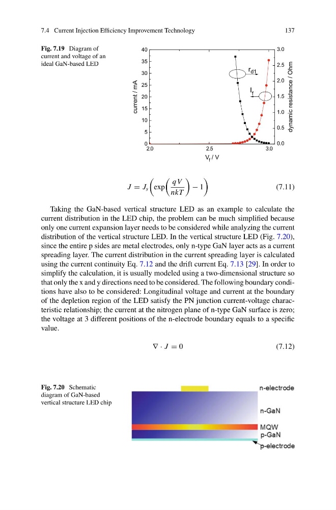
Fig. 7.19 Diagram of
current and voltage of an
ideal GaN-based LED
2.0
2.5
3.0
0
5
10
15
20
25
30
35
40
0.0
0.5
1.0
1.5
2.0
2.5
3.0
current / mA
V f / V
r d1
I f
dynamic resistance / Ohm
J = J s
exp
qV
nkT
− 1
(7.11)
Taking the GaN-based vertical structure LED as an example to calculate the
current distribution in the LED chip, the problem can be much simplified because
only one current expansion layer needs to be considered while analyzing the current
distribution of the vertical structure LED. In the vertical structure LED (Fig. 7.20),
since the entire p sides are metal electrodes, only n-type GaN layer acts as a current
spreading layer. The current distribution in the current spreading layer is calculated
using the current continuity Eq. 7.12 and the drift current Eq. 7.13 [29]. In order to
simplify the calculation, it is usually modeled using a two-dimensional structure so
that only the x and y directions need to be considered. The following boundary conditions have also to be considered: Longitudinal voltage and current at the boundary
of the depletion region of the LED satisfy the PN junction current-voltage characteristic relationship; the current at the nitrogen plane of n-type GaN surface is zero;
the voltage at 3 different positions of the n-electrode boundary equals to a specific
value.
∇ · J = 0
(7.12)
Fig. 7.20 Schematic
diagram of GaN-based
vertical structure LED chip
137
Fig. 7.19 Diagram of
current and voltage of an
ideal GaN-based LED
2.0
2.5
3.0
0
5
10
15
20
25
30
35
40
0.0
0.5
1.0
1.5
2.0
2.5
3.0
current / mA
V f / V
r d1
I f
dynamic resistance / Ohm
J = J s
exp
qV
nkT
− 1
(7.11)
Taking the GaN-based vertical structure LED as an example to calculate the
current distribution in the LED chip, the problem can be much simplified because
only one current expansion layer needs to be considered while analyzing the current
distribution of the vertical structure LED. In the vertical structure LED (Fig. 7.20),
since the entire p sides are metal electrodes, only n-type GaN layer acts as a current
spreading layer. The current distribution in the current spreading layer is calculated
using the current continuity Eq. 7.12 and the drift current Eq. 7.13 [29]. In order to
simplify the calculation, it is usually modeled using a two-dimensional structure so
that only the x and y directions need to be considered. The following boundary conditions have also to be considered: Longitudinal voltage and current at the boundary
of the depletion region of the LED satisfy the PN junction current-voltage characteristic relationship; the current at the nitrogen plane of n-type GaN surface is zero;
the voltage at 3 different positions of the n-electrode boundary equals to a specific
value.
∇ · J = 0
(7.12)
Fig. 7.20 Schematic
diagram of GaN-based
vertical structure LED chip