

7.3 Light Extraction Efficiency Improvement Technology
129
Fig. 7.14 250 nm diameter nanoarray by synchrotron radiation X-rays
LED on sapphire substrate. The sidewalls are modified to make it easier for photons
to escape. This will lead to much enhanced the light output power of LED.
GaN microporous etching techniques: To achieve an increase the light extraction
efficiency, LED chip surface can be also modified by nano-roughened. For instance,
the surface of the LED die is roughened by self-assembled CsCl nanospheres and
synchrotron radiation X-rays as shown in Fig. 7.14, which effectively improves the
light-emitting efficiency of the LED.
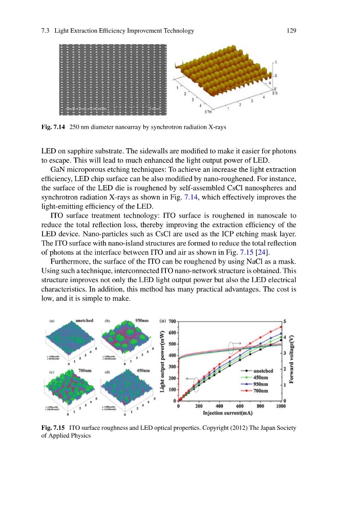
ITO surface treatment technology: ITO surface is roughened in nanoscale to
reduce the total reflection loss, thereby improving the extraction efficiency of the
LED device. Nano-particles such as CsCl are used as the ICP etching mask layer.
The ITO surface with nano-island structures are formed to reduce the total reflection
of photons at the interface between ITO and air as shown in Fig. 7.15 [24].
Furthermore, the surface of the ITO can be roughened by using NaCl as a mask.
Using such a technique, interconnected ITO nano-network structure is obtained. This
structure improves not only the LED light output power but also the LED electrical
characteristics. In addition, this method has many practical advantages. The cost is
low, and it is simple to make.
Fig. 7.15 ITO surface roughness and LED optical properties. Copyright (2012) The Japan Society
of Applied Physics
129
Fig. 7.14 250 nm diameter nanoarray by synchrotron radiation X-rays
LED on sapphire substrate. The sidewalls are modified to make it easier for photons
to escape. This will lead to much enhanced the light output power of LED.
GaN microporous etching techniques: To achieve an increase the light extraction
efficiency, LED chip surface can be also modified by nano-roughened. For instance,
the surface of the LED die is roughened by self-assembled CsCl nanospheres and
synchrotron radiation X-rays as shown in Fig. 7.14, which effectively improves the
light-emitting efficiency of the LED.
ITO surface treatment technology: ITO surface is roughened in nanoscale to
reduce the total reflection loss, thereby improving the extraction efficiency of the
LED device. Nano-particles such as CsCl are used as the ICP etching mask layer.
The ITO surface with nano-island structures are formed to reduce the total reflection
of photons at the interface between ITO and air as shown in Fig. 7.15 [24].
Furthermore, the surface of the ITO can be roughened by using NaCl as a mask.
Using such a technique, interconnected ITO nano-network structure is obtained. This
structure improves not only the LED light output power but also the LED electrical
characteristics. In addition, this method has many practical advantages. The cost is
low, and it is simple to make.
Fig. 7.15 ITO surface roughness and LED optical properties. Copyright (2012) The Japan Society
of Applied Physics