

7.1 Three Structures of LED
115
The difference between a flip-chip LED and a lateral structure LED is that the
light-emitting surface becomes a sapphire surface (there is also a sapphire substrate
removed, such as Osram’s thin film flip-chip LED), and the p-plane becomes a lightreflecting surface [4]. The LED chip is flip-bonded to another carrier substrate. This
carrier substrate may be a chip to improve the current drive circuit, cooling channels,
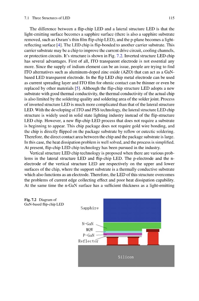
or protection circuits. It’s structure is shown in Fig. 7.2. Inverted structure LED chip
has several advantages. First of all, ITO transparent electrode is not essential any
more. Since the supply of indium element can be an issue, people are trying to find
ITO alternatives such as aluminum-doped zinc oxide (AZO) that can act as a GaNbased LED transparent electrode. In the flip LED chip metal electrode can be used
as current spreading layer and ITO film for ohmic contact can be thinner or even be
replaced by other materials [5]. Although the flip-chip structure LED adopts a new
substrate with good thermal conductivity, the thermal conductivity of the actual chip
is also limited by the soldering quality and soldering area of the solder joint. Process
of inverted structure LED is much more complicated than that of the lateral structure
LED. With the developing of ITO and PSS technology, the lateral structure LED chip
structure is widely used in solid state lighting industry instead of the flip-structure
LED chip. However, a new flip-chip LED process that does not require a substrate
is beginning to appear. This chip package does not require gold wire bonding, and
the chip is directly flipped on the package substrate by reflow or eutectic soldering.
Therefore, the direct contact area between the chip and the package substrate is large.
In this case, the heat dissipation problem is well solved, and the process is simplified.
At present, flip-chip LED chip technology has been pursued in the industry.
Vertical structure LED chip technology is proposed when there are various problems in the lateral structure LED and flip-chip LED. The p-electrode and the nelectrode of the vertical structure LED are respectively on the upper and lower
surfaces of the chip, where the support substrate is a thermally conductive substrate
which also functions as an electrode. Therefore, the LED of this structure overcomes
the problems of current edge collecting effect and poor heat dissipation capability.
At the same time the n-GaN surface has a sufficient thickness as a light-emitting
Fig. 7.2 Diagram of
GaN-based flip-chip LED
115
The difference between a flip-chip LED and a lateral structure LED is that the
light-emitting surface becomes a sapphire surface (there is also a sapphire substrate
removed, such as Osram’s thin film flip-chip LED), and the p-plane becomes a lightreflecting surface [4]. The LED chip is flip-bonded to another carrier substrate. This
carrier substrate may be a chip to improve the current drive circuit, cooling channels,
or protection circuits. It’s structure is shown in Fig. 7.2. Inverted structure LED chip
has several advantages. First of all, ITO transparent electrode is not essential any
more. Since the supply of indium element can be an issue, people are trying to find
ITO alternatives such as aluminum-doped zinc oxide (AZO) that can act as a GaNbased LED transparent electrode. In the flip LED chip metal electrode can be used
as current spreading layer and ITO film for ohmic contact can be thinner or even be
replaced by other materials [5]. Although the flip-chip structure LED adopts a new
substrate with good thermal conductivity, the thermal conductivity of the actual chip
is also limited by the soldering quality and soldering area of the solder joint. Process
of inverted structure LED is much more complicated than that of the lateral structure
LED. With the developing of ITO and PSS technology, the lateral structure LED chip
structure is widely used in solid state lighting industry instead of the flip-structure
LED chip. However, a new flip-chip LED process that does not require a substrate
is beginning to appear. This chip package does not require gold wire bonding, and
the chip is directly flipped on the package substrate by reflow or eutectic soldering.
Therefore, the direct contact area between the chip and the package substrate is large.
In this case, the heat dissipation problem is well solved, and the process is simplified.
At present, flip-chip LED chip technology has been pursued in the industry.
Vertical structure LED chip technology is proposed when there are various problems in the lateral structure LED and flip-chip LED. The p-electrode and the nelectrode of the vertical structure LED are respectively on the upper and lower
surfaces of the chip, where the support substrate is a thermally conductive substrate
which also functions as an electrode. Therefore, the LED of this structure overcomes
the problems of current edge collecting effect and poor heat dissipation capability.
At the same time the n-GaN surface has a sufficient thickness as a light-emitting
Fig. 7.2 Diagram of
GaN-based flip-chip LED