

114
7 III-Nitride LED Quantum Efficiency Improvement Technology
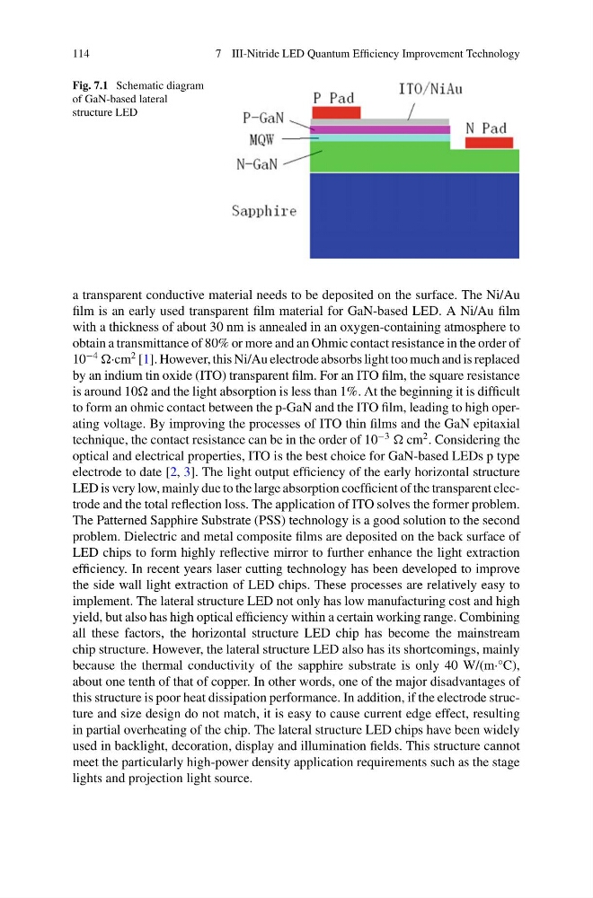
Fig. 7.1 Schematic diagram
of GaN-based lateral
structure LED
a transparent conductive material needs to be deposited on the surface. The Ni/Au
film is an early used transparent film material for GaN-based LED. A Ni/Au film
with a thickness of about 30 nm is annealed in an oxygen-containing atmosphere to
obtain a transmittance of 80% or more and an Ohmic contact resistance in the order of
10
−4
·cm
2 [1]. However, this Ni/Au electrode absorbs light too much and is replaced
by an indium tin oxide (ITO) transparent film. For an ITO film, the square resistance
is around 10 and the light absorption is less than 1%. At the beginning it is difficult
to form an ohmic contact between the p-GaN and the ITO film, leading to high operating voltage. By improving the processes of ITO thin films and the GaN epitaxial
technique, the contact resistance can be in the order of 10
−3
cm
2 . Considering the
optical and electrical properties, ITO is the best choice for GaN-based LEDs p type
electrode to date [2, 3]. The light output efficiency of the early horizontal structure
LED is very low, mainly due to the large absorption coefficient of the transparent electrode and the total reflection loss. The application of ITO solves the former problem.
The Patterned Sapphire Substrate (PSS) technology is a good solution to the second
problem. Dielectric and metal composite films are deposited on the back surface of
LED chips to form highly reflective mirror to further enhance the light extraction
efficiency. In recent years laser cutting technology has been developed to improve
the side wall light extraction of LED chips. These processes are relatively easy to
implement. The lateral structure LED not only has low manufacturing cost and high
yield, but also has high optical efficiency within a certain working range. Combining
all these factors, the horizontal structure LED chip has become the mainstream
chip structure. However, the lateral structure LED also has its shortcomings, mainly
because the thermal conductivity of the sapphire substrate is only 40 W/(m·°C),
about one tenth of that of copper. In other words, one of the major disadvantages of
this structure is poor heat dissipation performance. In addition, if the electrode structure and size design do not match, it is easy to cause current edge effect, resulting
in partial overheating of the chip. The lateral structure LED chips have been widely
used in backlight, decoration, display and illumination fields. This structure cannot
meet the particularly high-power density application requirements such as the stage
lights and projection light source.
7 III-Nitride LED Quantum Efficiency Improvement Technology
Fig. 7.1 Schematic diagram
of GaN-based lateral
structure LED
a transparent conductive material needs to be deposited on the surface. The Ni/Au
film is an early used transparent film material for GaN-based LED. A Ni/Au film
with a thickness of about 30 nm is annealed in an oxygen-containing atmosphere to
obtain a transmittance of 80% or more and an Ohmic contact resistance in the order of
10
−4
·cm
2 [1]. However, this Ni/Au electrode absorbs light too much and is replaced
by an indium tin oxide (ITO) transparent film. For an ITO film, the square resistance
is around 10 and the light absorption is less than 1%. At the beginning it is difficult
to form an ohmic contact between the p-GaN and the ITO film, leading to high operating voltage. By improving the processes of ITO thin films and the GaN epitaxial
technique, the contact resistance can be in the order of 10
−3
cm
2 . Considering the
optical and electrical properties, ITO is the best choice for GaN-based LEDs p type
electrode to date [2, 3]. The light output efficiency of the early horizontal structure
LED is very low, mainly due to the large absorption coefficient of the transparent electrode and the total reflection loss. The application of ITO solves the former problem.
The Patterned Sapphire Substrate (PSS) technology is a good solution to the second
problem. Dielectric and metal composite films are deposited on the back surface of
LED chips to form highly reflective mirror to further enhance the light extraction
efficiency. In recent years laser cutting technology has been developed to improve
the side wall light extraction of LED chips. These processes are relatively easy to
implement. The lateral structure LED not only has low manufacturing cost and high
yield, but also has high optical efficiency within a certain working range. Combining
all these factors, the horizontal structure LED chip has become the mainstream
chip structure. However, the lateral structure LED also has its shortcomings, mainly
because the thermal conductivity of the sapphire substrate is only 40 W/(m·°C),
about one tenth of that of copper. In other words, one of the major disadvantages of
this structure is poor heat dissipation performance. In addition, if the electrode structure and size design do not match, it is easy to cause current edge effect, resulting
in partial overheating of the chip. The lateral structure LED chips have been widely
used in backlight, decoration, display and illumination fields. This structure cannot
meet the particularly high-power density application requirements such as the stage
lights and projection light source.