

13 Creation of Organic-Metal Hybridized Nanocrystals …
259
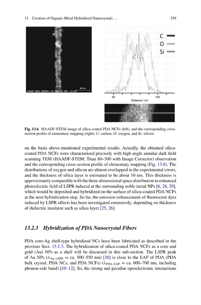
Fig. 13.6 HAADF-STEM image of silica-coated PDA NCFs (left), and the corresponding crosssection profile of elementary mapping (right). C: carbon, O: oxygen, and Si: silicon
on the basis above-mentioned experimental results. Actually, the obtained silicacoated PDA NCFs were characterized precisely with high-angle annular dark field
scanning TEM (HAADF-STEM: Titan 80–300 with Image Corrector) observation
and the corresponding cross-section profile of elementary mapping (Fig. 13.6). The
distributions of oxygen and silicon are almost overlapped in the experimental errors,
and the thickness of silica layer is estimated to be about 10 nm. This thickness is
approximately comparable with the three-dimensional space distribution in enhanced
photoelectric field of LSPR induced at the surrounding noble metal NPs [6, 28, 29],
which would be deposited and hybridized on the surface of silica-coated PDA NCFs
at the next hybridization step. So far, the emission enhancement of fluorescent dyes
induced by LSPR effects has been investigated extensively, depending on thickness
of dielectric insulator such as silica layer [25, 26].
13.2.3 Hybridization of PDA Nanocrystal Fibers
PDA core-Ag shell-type hybridized NCs have been fabricated as described in the
previous Sect. 13.1.3. The hybridization of silica-coated PDA NCFs as a core and
gold (Au) NPs as a shell will be discussed in this sub-section. The LSPR peak
of Au NPs (λ Au, LSPR = ca. 500–550 nm) [30] is close to the EAP of PDA (PDA
bulk crystal, PDA NCs, and PDA NCFs) (λ PDA, EAP = ca. 600–700 nm, including
phonon-side band) [10–12]. So, the strong and peculiar optoelectronic interactions
259
Fig. 13.6 HAADF-STEM image of silica-coated PDA NCFs (left), and the corresponding crosssection profile of elementary mapping (right). C: carbon, O: oxygen, and Si: silicon
on the basis above-mentioned experimental results. Actually, the obtained silicacoated PDA NCFs were characterized precisely with high-angle annular dark field
scanning TEM (HAADF-STEM: Titan 80–300 with Image Corrector) observation
and the corresponding cross-section profile of elementary mapping (Fig. 13.6). The
distributions of oxygen and silicon are almost overlapped in the experimental errors,
and the thickness of silica layer is estimated to be about 10 nm. This thickness is
approximately comparable with the three-dimensional space distribution in enhanced
photoelectric field of LSPR induced at the surrounding noble metal NPs [6, 28, 29],
which would be deposited and hybridized on the surface of silica-coated PDA NCFs
at the next hybridization step. So far, the emission enhancement of fluorescent dyes
induced by LSPR effects has been investigated extensively, depending on thickness
of dielectric insulator such as silica layer [25, 26].
13.2.3 Hybridization of PDA Nanocrystal Fibers
PDA core-Ag shell-type hybridized NCs have been fabricated as described in the
previous Sect. 13.1.3. The hybridization of silica-coated PDA NCFs as a core and
gold (Au) NPs as a shell will be discussed in this sub-section. The LSPR peak
of Au NPs (λ Au, LSPR = ca. 500–550 nm) [30] is close to the EAP of PDA (PDA
bulk crystal, PDA NCs, and PDA NCFs) (λ PDA, EAP = ca. 600–700 nm, including
phonon-side band) [10–12]. So, the strong and peculiar optoelectronic interactions