

Analysis of InN-Based Surrounded Gate Tunnel …
79
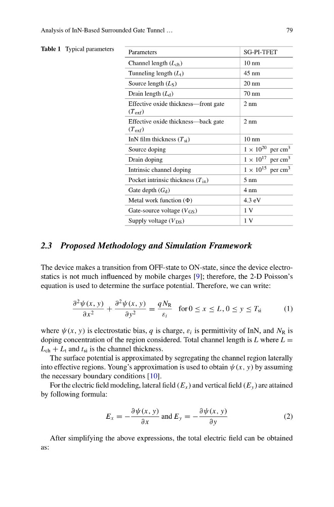
Table 1 Typical parameters
Parameters
SG-PI-TFET
Channel length (L ch )
10 nm
Tunneling length (L t )
45 nm
Source length (L S )
20 nm
Drain length (L d )
70 nm
Effective oxide thickness—front gate
(T oxf )
2 nm
Effective oxide thickness—back gate
(T oxf )
2 nm
InN film thickness (T si )
10 nm
Source doping
1 × 10 20 per cm 3
Drain doping
1 × 10 17 per cm 3
Intrinsic channel doping
1 × 10 15 per cm 3
Pocket intrinsic thickness (T in )
5 nm
Gate depth (G d )
4 nm
Metal work function ()
4.3 eV
Gate-source voltage (V GS )
1 V
Supply voltage (V DS )
1 V
2.3 Proposed Methodology and Simulation Framework
The device makes a transition from OFF-state to ON-state, since the device electrostatics is not much influenced by mobile charges [9]; therefore, the 2-D Poisson’s
equation is used to determine the surface potential. Therefore, we can write:
∂
2
ψ(x, y)
∂ x 2
+
∂
2
ψ(x, y)
∂ y 2
=
q N R
ε i
for 0 ≤ x ≤ L , 0 ≤ y ≤ T si
(1)
where ψ(x, y) is electrostatic bias, q is charge, ε i is permittivity of InN, and N R is
doping concentration of the region considered. Total channel length is L where L =
L ch + L t and t si is the channel thickness.
The surface potential is approximated by segregating the channel region laterally
into effective regions. Young’s approximation is used to obtain ψ(x, y) by assuming
the necessary boundary conditions [10].
For the electric field modeling, lateral field (E x ) and vertical field (E y ) are attained
by following formula:
E x = −
∂ψ(x, y)
∂ x
and E y = −
∂ψ(x, y)
∂ y
(2)
After simplifying the above expressions, the total electric field can be obtained
as:
79
Table 1 Typical parameters
Parameters
SG-PI-TFET
Channel length (L ch )
10 nm
Tunneling length (L t )
45 nm
Source length (L S )
20 nm
Drain length (L d )
70 nm
Effective oxide thickness—front gate
(T oxf )
2 nm
Effective oxide thickness—back gate
(T oxf )
2 nm
InN film thickness (T si )
10 nm
Source doping
1 × 10 20 per cm 3
Drain doping
1 × 10 17 per cm 3
Intrinsic channel doping
1 × 10 15 per cm 3
Pocket intrinsic thickness (T in )
5 nm
Gate depth (G d )
4 nm
Metal work function ()
4.3 eV
Gate-source voltage (V GS )
1 V
Supply voltage (V DS )
1 V
2.3 Proposed Methodology and Simulation Framework
The device makes a transition from OFF-state to ON-state, since the device electrostatics is not much influenced by mobile charges [9]; therefore, the 2-D Poisson’s
equation is used to determine the surface potential. Therefore, we can write:
∂
2
ψ(x, y)
∂ x 2
+
∂
2
ψ(x, y)
∂ y 2
=
q N R
ε i
for 0 ≤ x ≤ L , 0 ≤ y ≤ T si
(1)
where ψ(x, y) is electrostatic bias, q is charge, ε i is permittivity of InN, and N R is
doping concentration of the region considered. Total channel length is L where L =
L ch + L t and t si is the channel thickness.
The surface potential is approximated by segregating the channel region laterally
into effective regions. Young’s approximation is used to obtain ψ(x, y) by assuming
the necessary boundary conditions [10].
For the electric field modeling, lateral field (E x ) and vertical field (E y ) are attained
by following formula:
E x = −
∂ψ(x, y)
∂ x
and E y = −
∂ψ(x, y)
∂ y
(2)
After simplifying the above expressions, the total electric field can be obtained
as: