

78
R. Dutta and N. Paitya
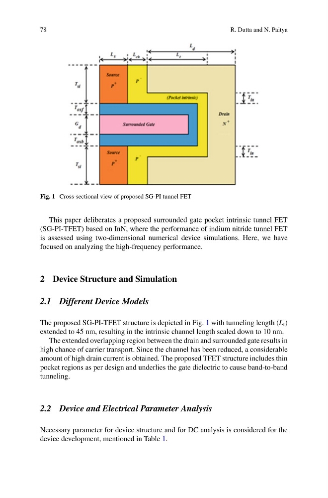
Fig. 1 Cross-sectional view of proposed SG-PI tunnel FET
This paper deliberates a proposed surrounded gate pocket intrinsic tunnel FET
(SG-PI-TFET) based on InN, where the performance of indium nitride tunnel FET
is assessed using two-dimensional numerical device simulations. Here, we have
focused on analyzing the high-frequency performance.
2 Device Structure and Simulation
2.1 Different Device Models
The proposed SG-PI-TFET structure is depicted in Fig. 1 with tunneling length (L t )
extended to 45 nm, resulting in the intrinsic channel length scaled down to 10 nm.
The extended overlapping region between the drain and surrounded gate results in
high chance of carrier transport. Since the channel has been reduced, a considerable
amount of high drain current is obtained. The proposed TFET structure includes thin
pocket regions as per design and underlies the gate dielectric to cause band-to-band
tunneling.
2.2 Device and Electrical Parameter Analysis
Necessary parameter for device structure and for DC analysis is considered for the
device development, mentioned in Table 1.
R. Dutta and N. Paitya
Fig. 1 Cross-sectional view of proposed SG-PI tunnel FET
This paper deliberates a proposed surrounded gate pocket intrinsic tunnel FET
(SG-PI-TFET) based on InN, where the performance of indium nitride tunnel FET
is assessed using two-dimensional numerical device simulations. Here, we have
focused on analyzing the high-frequency performance.
2 Device Structure and Simulation
2.1 Different Device Models
The proposed SG-PI-TFET structure is depicted in Fig. 1 with tunneling length (L t )
extended to 45 nm, resulting in the intrinsic channel length scaled down to 10 nm.
The extended overlapping region between the drain and surrounded gate results in
high chance of carrier transport. Since the channel has been reduced, a considerable
amount of high drain current is obtained. The proposed TFET structure includes thin
pocket regions as per design and underlies the gate dielectric to cause band-to-band
tunneling.
2.2 Device and Electrical Parameter Analysis
Necessary parameter for device structure and for DC analysis is considered for the
device development, mentioned in Table 1.