

RF Performance of Ultra-wide Band Gap HEMTs
57
Further optimization is expected due to ongoing reporting of devices having lower
values of on-resistance (R ON ), contact resistance (R C ), and sheet-resistance (R SH );
there are tangible benefits of significant improvements in power switching and RF
performance of devices: reduced size of passive components and so small device
size, and facilitate integration of both hybrid and monolithic RF and robust switch
technology [56].
Comparison of large signal CW and pulsed RF performance of β-Ga 2 O 3 fieldplated MOSFETs demonstrated by Singh et al. [57], and highlighted benefit of pulsed
signal circumventing device heating; poor heat dissipation of Ga 2 O 3 devices restricts
high-voltage operations as thermal conductivity of Ga 2 O 3 material is very low
(~0.2 W cm
−1 K
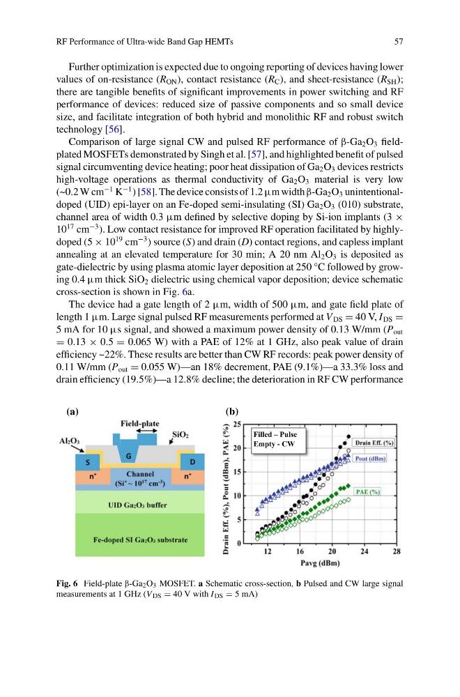
−1 ) [58]. The device consists of 1.2 μm width β-Ga 2 O 3 unintentionaldoped (UID) epi-layer on an Fe-doped semi-insulating (SI) Ga 2 O 3 (010) substrate,
channel area of width 0.3 μm defined by selective doping by Si-ion implants (3 ×
10
17 cm
−3 ). Low contact resistance for improved RF operation facilitated by highlydoped (5 × 10
19 cm
−3 ) source (S) and drain (D) contact regions, and capless implant
annealing at an elevated temperature for 30 min; A 20 nm Al 2 O 3 is deposited as
gate-dielectric by using plasma atomic layer deposition at 250 °C followed by growing 0.4 μm thick SiO 2 dielectric using chemical vapor deposition; device schematic
cross-section is shown in Fig. 6a.
The device had a gate length of 2 μm, width of 500 μm, and gate field plate of
length 1 μm. Large signal pulsed RF measurements performed at V DS = 40 V, I DS =
5 mA for 10 μs signal, and showed a maximum power density of 0.13 W/mm (P out
= 0.13 × 0.5 = 0.065 W) with a PAE of 12% at 1 GHz, also peak value of drain
efficiency ~22%. These results are better than CW RF records: peak power density of
0.11 W/mm (P out = 0.055 W)—an 18% decrement, PAE (9.1%)—a 33.3% loss and
drain efficiency (19.5%)—a 12.8% decline; the deterioration in RF CW performance
Filled – Pulse
Empty - CW
(a)
(b)
Fig. 6 Field-plate β-Ga 2 O 3 MOSFET. a Schematic cross-section, b Pulsed and CW large signal
measurements at 1 GHz (V DS = 40 V with I DS = 5 mA)
57
Further optimization is expected due to ongoing reporting of devices having lower
values of on-resistance (R ON ), contact resistance (R C ), and sheet-resistance (R SH );
there are tangible benefits of significant improvements in power switching and RF
performance of devices: reduced size of passive components and so small device
size, and facilitate integration of both hybrid and monolithic RF and robust switch
technology [56].
Comparison of large signal CW and pulsed RF performance of β-Ga 2 O 3 fieldplated MOSFETs demonstrated by Singh et al. [57], and highlighted benefit of pulsed
signal circumventing device heating; poor heat dissipation of Ga 2 O 3 devices restricts
high-voltage operations as thermal conductivity of Ga 2 O 3 material is very low
(~0.2 W cm
−1 K
−1 ) [58]. The device consists of 1.2 μm width β-Ga 2 O 3 unintentionaldoped (UID) epi-layer on an Fe-doped semi-insulating (SI) Ga 2 O 3 (010) substrate,
channel area of width 0.3 μm defined by selective doping by Si-ion implants (3 ×
10
17 cm
−3 ). Low contact resistance for improved RF operation facilitated by highlydoped (5 × 10
19 cm
−3 ) source (S) and drain (D) contact regions, and capless implant
annealing at an elevated temperature for 30 min; A 20 nm Al 2 O 3 is deposited as
gate-dielectric by using plasma atomic layer deposition at 250 °C followed by growing 0.4 μm thick SiO 2 dielectric using chemical vapor deposition; device schematic
cross-section is shown in Fig. 6a.
The device had a gate length of 2 μm, width of 500 μm, and gate field plate of
length 1 μm. Large signal pulsed RF measurements performed at V DS = 40 V, I DS =
5 mA for 10 μs signal, and showed a maximum power density of 0.13 W/mm (P out
= 0.13 × 0.5 = 0.065 W) with a PAE of 12% at 1 GHz, also peak value of drain
efficiency ~22%. These results are better than CW RF records: peak power density of
0.11 W/mm (P out = 0.055 W)—an 18% decrement, PAE (9.1%)—a 33.3% loss and
drain efficiency (19.5%)—a 12.8% decline; the deterioration in RF CW performance
Filled – Pulse
Empty - CW
(a)
(b)
Fig. 6 Field-plate β-Ga 2 O 3 MOSFET. a Schematic cross-section, b Pulsed and CW large signal
measurements at 1 GHz (V DS = 40 V with I DS = 5 mA)