

58
R. Singh et al.
mainly due to self-heating: channel temperature during CW RF is 58 °C while 28 °C
for pulsed RF. Large signal CW and pulsed RF performance of the device are shown
in Fig. 6b.
4 Limits to RF and DC Performance (GaN and Ga 2 O 3
HEMTs)
Prospective RF and DC power applications of HEMTs beg the question asking for
suitability of GaN or Ga 2 O 3 devices; the question is addressed by Kumar et al.
[59], and stated that β-Ga 2 O 3 HEMTs can deliver more RF output power over GaN
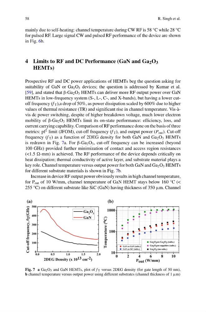
HEMTs in low-frequency system (S-, L-, C-, and X-bands), but having a lower cutoff frequency (f T ),a drop of 50%, as power dissipation scaled by 600% due to higher
values of thermal resistance (TR) and significant rise in channel temperature. Vis-àvis dc power switching, despite of higher breakdown voltage, much lower electron
mobility of β-Ga 2 O 3 HEMTs limit its on-state performance: efficiency, loss, and
current carrying capability. Comparison of RF performance done on the basis of three
metrics: pf
2 limit (JFOM), cut-off frequency (f T ), and output power (P out ). Cut-off
frequency (f T ) as a function of 2DEG density for both GaN and Ga 2 O 3 HEMTs
is redrawn in Fig. 7a. For β-Ga 2 O 3 , cut-off frequency can be increased (beyond
100 GHz) provided further minimization of contact and access region resistances
(<1.5 -mm) is achieved. The RF performance of the device depends critically on
heat dissipation; thermal conductivity of active layer, and substrate material plays a
key role. Channel temperature versus output power for both GaN and Ga 2 O 3 HEMTs
for different substrate materials is shown in Fig. 7b.
Increase in device RF output power obviously results in high channel temperature,
for P out of 10 W/mm, channel temperature of GaN HEMT stays below 160 °C (<
255 °C) on different substrate like SiC (GaN) having thickness of 350 μm. Channel
Fig. 7 a Ga 2 O 3 and GaN HEMTs, plot of f T versus 2DEG density (for gate length of 50 nm),
b channel temperature versus output power using different substrates (channel thickness of 1 μm)
R. Singh et al.
mainly due to self-heating: channel temperature during CW RF is 58 °C while 28 °C
for pulsed RF. Large signal CW and pulsed RF performance of the device are shown
in Fig. 6b.
4 Limits to RF and DC Performance (GaN and Ga 2 O 3
HEMTs)
Prospective RF and DC power applications of HEMTs beg the question asking for
suitability of GaN or Ga 2 O 3 devices; the question is addressed by Kumar et al.
[59], and stated that β-Ga 2 O 3 HEMTs can deliver more RF output power over GaN
HEMTs in low-frequency system (S-, L-, C-, and X-bands), but having a lower cutoff frequency (f T ),a drop of 50%, as power dissipation scaled by 600% due to higher
values of thermal resistance (TR) and significant rise in channel temperature. Vis-àvis dc power switching, despite of higher breakdown voltage, much lower electron
mobility of β-Ga 2 O 3 HEMTs limit its on-state performance: efficiency, loss, and
current carrying capability. Comparison of RF performance done on the basis of three
metrics: pf
2 limit (JFOM), cut-off frequency (f T ), and output power (P out ). Cut-off
frequency (f T ) as a function of 2DEG density for both GaN and Ga 2 O 3 HEMTs
is redrawn in Fig. 7a. For β-Ga 2 O 3 , cut-off frequency can be increased (beyond
100 GHz) provided further minimization of contact and access region resistances
(<1.5 -mm) is achieved. The RF performance of the device depends critically on
heat dissipation; thermal conductivity of active layer, and substrate material plays a
key role. Channel temperature versus output power for both GaN and Ga 2 O 3 HEMTs
for different substrate materials is shown in Fig. 7b.
Increase in device RF output power obviously results in high channel temperature,
for P out of 10 W/mm, channel temperature of GaN HEMT stays below 160 °C (<
255 °C) on different substrate like SiC (GaN) having thickness of 350 μm. Channel
Fig. 7 a Ga 2 O 3 and GaN HEMTs, plot of f T versus 2DEG density (for gate length of 50 nm),
b channel temperature versus output power using different substrates (channel thickness of 1 μm)