

56
R. Singh et al.
RF switches. Furthermore, high-speed E-/D-mode GaN HEMTs can be integrated
to realize complex circuits ranging from mixed signal to digital logic [8].
3 RF Performance of β-Ga 2 O 3 Devices
Current trend of research of Ga 2 O 3 device technology is already in a fast lane and
achieving key milestones [51–54] supported by adequate process development and
vital material advancement. Excellent material characteristics of β-Ga 2 O 3 enabled
high value of JFOM (40, Table 1)—Johnson’s FOM—a important parameter describing power-frequency product for RF operation, paved the way for β-Ga 2 O 3 transistors
to operate as high-efficiency RF power amplifiers, RF switches, and power switches
capable of GHz switching speeds [8]. Also large bandgap (E g ~4.9 eV) enabled high
value of breakdown field (E Br ~8 MV cm
−1 ) of β-Ga 2 O 3, facilitated higher values of
almost all FOMs: JFOM (∝E Br ), BFOM (∝E
3
Br ), and BHFFOM (∝E
2
Br ), thus finds
suitable for power switching and RF applications.
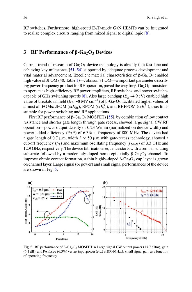
First RF performance of β-Ga 2 O 3 MOSFETs [55], by combination of low contact
resistance and shorter gate length through gate recess, showed large signal CW RF
operation—power output density of 0.23 W/mm (normalized on device width) and
power added efficiency (PAE) of 6.3% at frequency of 800 MHz. The device had
a gate length of 0.7 μm, width 2 × 50 μm with gate-recess technology, showed a
cut-off frequency (f T ) and maximum oscillating frequency (f MAX ) of 3.3 GHz and
12.9 GHz, respectively. The device fabrication sequence starts with a semi-insulating
substrate followed by a moderately doped homo-epitaxially β-Ga 2 O 3 channel. To
improve ohmic contact formation, a thin highly-doped β-Ga 2 O 3 cap layer is grown
on channel layer. Large signal (or power) and small signal performances of the device
are shown in Fig. 5.
f max = 12.9 GHz
f T = 3.3 GHz
∪
ℎ 21
2
L g = 0.7 μm
W = 100 μm
V DS = 25 V
(a)
(b)
Fig. 5 RF performance of β-Ga 2 O 3 MOSFET. a Large signal CW output power (13.7 dBm), gain
(5.1 dB), and PAE MAX (6.3%) versus input power (P in ) at 800 MHz, b small signal gain as a function
of operating frequency
R. Singh et al.
RF switches. Furthermore, high-speed E-/D-mode GaN HEMTs can be integrated
to realize complex circuits ranging from mixed signal to digital logic [8].
3 RF Performance of β-Ga 2 O 3 Devices
Current trend of research of Ga 2 O 3 device technology is already in a fast lane and
achieving key milestones [51–54] supported by adequate process development and
vital material advancement. Excellent material characteristics of β-Ga 2 O 3 enabled
high value of JFOM (40, Table 1)—Johnson’s FOM—a important parameter describing power-frequency product for RF operation, paved the way for β-Ga 2 O 3 transistors
to operate as high-efficiency RF power amplifiers, RF switches, and power switches
capable of GHz switching speeds [8]. Also large bandgap (E g ~4.9 eV) enabled high
value of breakdown field (E Br ~8 MV cm
−1 ) of β-Ga 2 O 3, facilitated higher values of
almost all FOMs: JFOM (∝E Br ), BFOM (∝E
3
Br ), and BHFFOM (∝E
2
Br ), thus finds
suitable for power switching and RF applications.
First RF performance of β-Ga 2 O 3 MOSFETs [55], by combination of low contact
resistance and shorter gate length through gate recess, showed large signal CW RF
operation—power output density of 0.23 W/mm (normalized on device width) and
power added efficiency (PAE) of 6.3% at frequency of 800 MHz. The device had
a gate length of 0.7 μm, width 2 × 50 μm with gate-recess technology, showed a
cut-off frequency (f T ) and maximum oscillating frequency (f MAX ) of 3.3 GHz and
12.9 GHz, respectively. The device fabrication sequence starts with a semi-insulating
substrate followed by a moderately doped homo-epitaxially β-Ga 2 O 3 channel. To
improve ohmic contact formation, a thin highly-doped β-Ga 2 O 3 cap layer is grown
on channel layer. Large signal (or power) and small signal performances of the device
are shown in Fig. 5.
f max = 12.9 GHz
f T = 3.3 GHz
∪
ℎ 21
2
L g = 0.7 μm
W = 100 μm
V DS = 25 V
(a)
(b)
Fig. 5 RF performance of β-Ga 2 O 3 MOSFET. a Large signal CW output power (13.7 dBm), gain
(5.1 dB), and PAE MAX (6.3%) versus input power (P in ) at 800 MHz, b small signal gain as a function
of operating frequency