

200
B. Choudhuri and A. Mondal
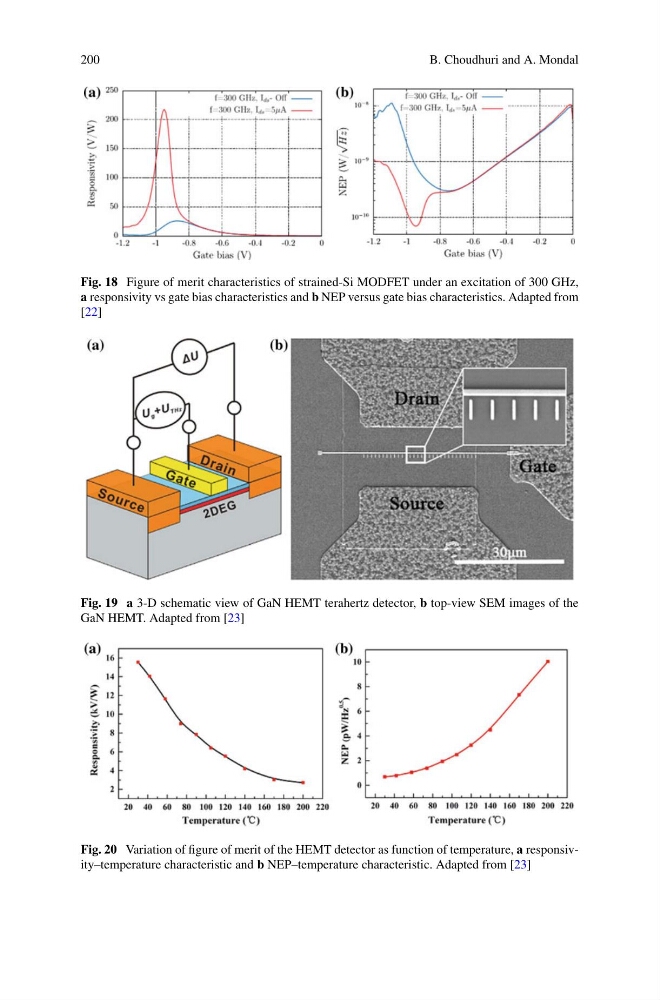
Fig. 18 Figure of merit characteristics of strained-Si MODFET under an excitation of 300 GHz,
a responsivity vs gate bias characteristics and b NEP versus gate bias characteristics. Adapted from
[22]
Fig. 19 a 3-D schematic view of GaN HEMT terahertz detector, b top-view SEM images of the
GaN HEMT. Adapted from [23]
Fig. 20 Variation of figure of merit of the HEMT detector as function of temperature, a responsivity–temperature characteristic and b NEP–temperature characteristic. Adapted from [23]
B. Choudhuri and A. Mondal
Fig. 18 Figure of merit characteristics of strained-Si MODFET under an excitation of 300 GHz,
a responsivity vs gate bias characteristics and b NEP versus gate bias characteristics. Adapted from
[22]
Fig. 19 a 3-D schematic view of GaN HEMT terahertz detector, b top-view SEM images of the
GaN HEMT. Adapted from [23]
Fig. 20 Variation of figure of merit of the HEMT detector as function of temperature, a responsivity–temperature characteristic and b NEP–temperature characteristic. Adapted from [23]