

Group III—Nitrides and Other Semiconductors for Terahertz Detector
199
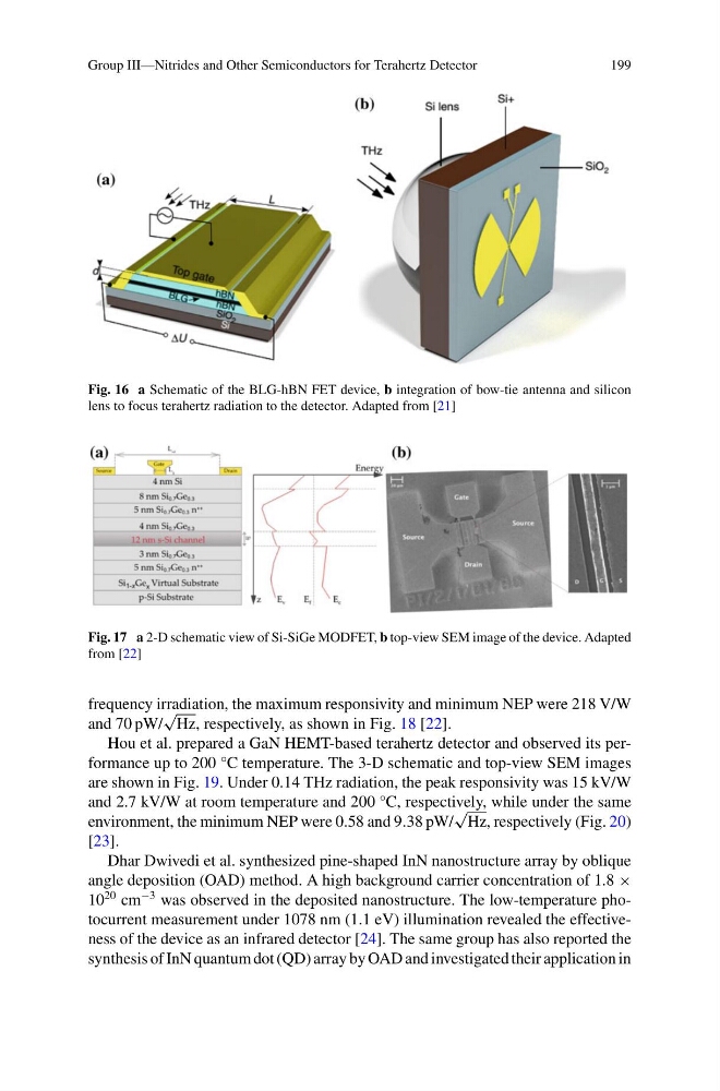
Fig. 16 a Schematic of the BLG-hBN FET device, b integration of bow-tie antenna and silicon
lens to focus terahertz radiation to the detector. Adapted from [21]
Fig. 17 a 2-D schematic view of Si-SiGe MODFET, b top-view SEM image of the device. Adapted
from [22]
frequency irradiation, the maximum responsivity and minimum NEP were 218 V/W
and 70 pW/
√
Hz, respectively, as shown in Fig. 18 [22].
Hou et al. prepared a GaN HEMT-based terahertz detector and observed its performance up to 200 °C temperature. The 3-D schematic and top-view SEM images
are shown in Fig. 19. Under 0.14 THz radiation, the peak responsivity was 15 kV/W
and 2.7 kV/W at room temperature and 200 °C, respectively, while under the same
environment, the minimum NEP were 0.58 and 9.38 pW/
√
Hz, respectively (Fig. 20)
[23].
Dhar Dwivedi et al. synthesized pine-shaped InN nanostructure array by oblique
angle deposition (OAD) method. A high background carrier concentration of 1.8 ×
10
20 cm
−3 was observed in the deposited nanostructure. The low-temperature photocurrent measurement under 1078 nm (1.1 eV) illumination revealed the effectiveness of the device as an infrared detector [24]. The same group has also reported the
synthesis of InN quantum dot (QD) array by OAD and investigated their application in
199
Fig. 16 a Schematic of the BLG-hBN FET device, b integration of bow-tie antenna and silicon
lens to focus terahertz radiation to the detector. Adapted from [21]
Fig. 17 a 2-D schematic view of Si-SiGe MODFET, b top-view SEM image of the device. Adapted
from [22]
frequency irradiation, the maximum responsivity and minimum NEP were 218 V/W
and 70 pW/
√
Hz, respectively, as shown in Fig. 18 [22].
Hou et al. prepared a GaN HEMT-based terahertz detector and observed its performance up to 200 °C temperature. The 3-D schematic and top-view SEM images
are shown in Fig. 19. Under 0.14 THz radiation, the peak responsivity was 15 kV/W
and 2.7 kV/W at room temperature and 200 °C, respectively, while under the same
environment, the minimum NEP were 0.58 and 9.38 pW/
√
Hz, respectively (Fig. 20)
[23].
Dhar Dwivedi et al. synthesized pine-shaped InN nanostructure array by oblique
angle deposition (OAD) method. A high background carrier concentration of 1.8 ×
10
20 cm
−3 was observed in the deposited nanostructure. The low-temperature photocurrent measurement under 1078 nm (1.1 eV) illumination revealed the effectiveness of the device as an infrared detector [24]. The same group has also reported the
synthesis of InN quantum dot (QD) array by OAD and investigated their application in