

198
B. Choudhuri and A. Mondal
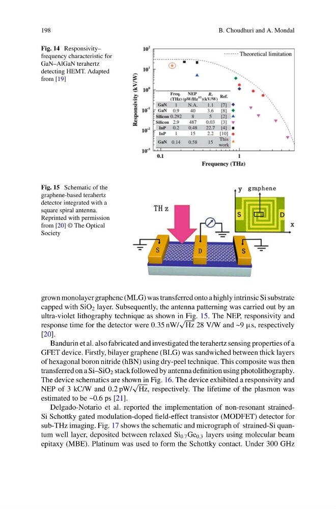
Fig. 14 Responsivity–
frequency characteristic for
GaN–AlGaN terahertz
detecting HEMT. Adapted
from [19]
Fig. 15 Schematic of the
graphene-based terahertz
detector integrated with a
square spiral antenna.
Reprinted with permission
from [20] © The Optical
Society
grown monolayer graphene (MLG) was transferred onto a highly intrinsic Si substrate
capped with SiO 2 layer. Subsequently, the antenna patterning was carried out by an
ultra-violet lithography technique as shown in Fig. 15. The NEP, responsivity and
response time for the detector were 0.35 nW/
√
Hz 28 V/W and ~9 µs, respectively
[20].
Bandurin et al. also fabricated and investigated the terahertz sensing properties of a
GFET device. Firstly, bilayer graphene (BLG) was sandwiched between thick layers
of hexagonal boron nitride (hBN) using dry-peel technique. This composite was then
transferred on a Si–SiO 2 stack followed by antenna definition using photolithography.
The device schematics are shown in Fig. 16. The device exhibited a responsivity and
NEP of 3 kC/W and 0.2 pW/
√
Hz, respectively. The lifetime of the plasmon was
estimated to be ~0.6 ps [21].
Delgado-Notario et al. reported the implementation of non-resonant strainedSi Schottky gated modulation-doped field-effect transistor (MODFET) detector for
sub-THz imaging. Fig. 17 shows the schematic and micrograph of strained-Si quantum well layer, deposited between relaxed Si 0.7 Ge 0.3 layers using molecular beam
epitaxy (MBE). Platinum was used to form the Schottky contact. Under 300 GHz
B. Choudhuri and A. Mondal
Fig. 14 Responsivity–
frequency characteristic for
GaN–AlGaN terahertz
detecting HEMT. Adapted
from [19]
Fig. 15 Schematic of the
graphene-based terahertz
detector integrated with a
square spiral antenna.
Reprinted with permission
from [20] © The Optical
Society
grown monolayer graphene (MLG) was transferred onto a highly intrinsic Si substrate
capped with SiO 2 layer. Subsequently, the antenna patterning was carried out by an
ultra-violet lithography technique as shown in Fig. 15. The NEP, responsivity and
response time for the detector were 0.35 nW/
√
Hz 28 V/W and ~9 µs, respectively
[20].
Bandurin et al. also fabricated and investigated the terahertz sensing properties of a
GFET device. Firstly, bilayer graphene (BLG) was sandwiched between thick layers
of hexagonal boron nitride (hBN) using dry-peel technique. This composite was then
transferred on a Si–SiO 2 stack followed by antenna definition using photolithography.
The device schematics are shown in Fig. 16. The device exhibited a responsivity and
NEP of 3 kC/W and 0.2 pW/
√
Hz, respectively. The lifetime of the plasmon was
estimated to be ~0.6 ps [21].
Delgado-Notario et al. reported the implementation of non-resonant strainedSi Schottky gated modulation-doped field-effect transistor (MODFET) detector for
sub-THz imaging. Fig. 17 shows the schematic and micrograph of strained-Si quantum well layer, deposited between relaxed Si 0.7 Ge 0.3 layers using molecular beam
epitaxy (MBE). Platinum was used to form the Schottky contact. Under 300 GHz