

Group III—Nitrides and Other Semiconductors for Terahertz Detector
197
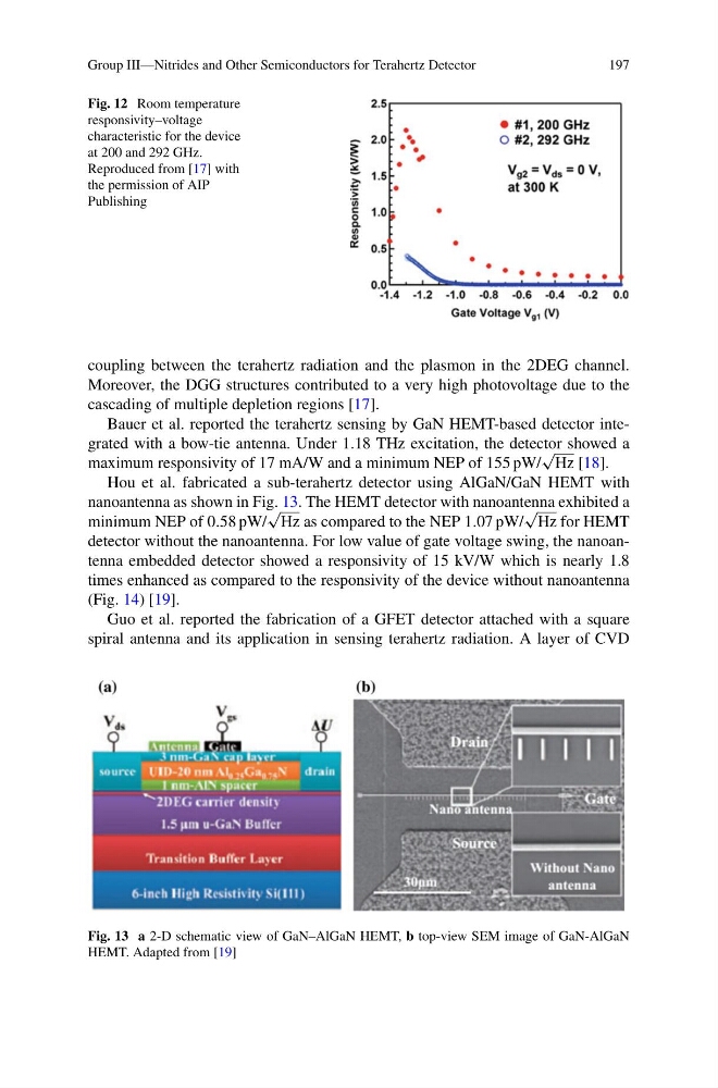
Fig. 12 Room temperature
responsivity–voltage
characteristic for the device
at 200 and 292 GHz.
Reproduced from [17] with
the permission of AIP
Publishing
coupling between the terahertz radiation and the plasmon in the 2DEG channel.
Moreover, the DGG structures contributed to a very high photovoltage due to the
cascading of multiple depletion regions [17].
Bauer et al. reported the terahertz sensing by GaN HEMT-based detector integrated with a bow-tie antenna. Under 1.18 THz excitation, the detector showed a
maximum responsivity of 17 mA/W and a minimum NEP of 155 pW/
√
Hz [18].
Hou et al. fabricated a sub-terahertz detector using AlGaN/GaN HEMT with
nanoantenna as shown in Fig. 13. The HEMT detector with nanoantenna exhibited a
minimum NEP of 0.58 pW/
√
Hz as compared to the NEP 1.07 pW/
√
Hz for HEMT
detector without the nanoantenna. For low value of gate voltage swing, the nanoantenna embedded detector showed a responsivity of 15 kV/W which is nearly 1.8
times enhanced as compared to the responsivity of the device without nanoantenna
(Fig. 14) [19].
Guo et al. reported the fabrication of a GFET detector attached with a square
spiral antenna and its application in sensing terahertz radiation. A layer of CVD
Fig. 13 a 2-D schematic view of GaN–AlGaN HEMT, b top-view SEM image of GaN-AlGaN
HEMT. Adapted from [19]
197
Fig. 12 Room temperature
responsivity–voltage
characteristic for the device
at 200 and 292 GHz.
Reproduced from [17] with
the permission of AIP
Publishing
coupling between the terahertz radiation and the plasmon in the 2DEG channel.
Moreover, the DGG structures contributed to a very high photovoltage due to the
cascading of multiple depletion regions [17].
Bauer et al. reported the terahertz sensing by GaN HEMT-based detector integrated with a bow-tie antenna. Under 1.18 THz excitation, the detector showed a
maximum responsivity of 17 mA/W and a minimum NEP of 155 pW/
√
Hz [18].
Hou et al. fabricated a sub-terahertz detector using AlGaN/GaN HEMT with
nanoantenna as shown in Fig. 13. The HEMT detector with nanoantenna exhibited a
minimum NEP of 0.58 pW/
√
Hz as compared to the NEP 1.07 pW/
√
Hz for HEMT
detector without the nanoantenna. For low value of gate voltage swing, the nanoantenna embedded detector showed a responsivity of 15 kV/W which is nearly 1.8
times enhanced as compared to the responsivity of the device without nanoantenna
(Fig. 14) [19].
Guo et al. reported the fabrication of a GFET detector attached with a square
spiral antenna and its application in sensing terahertz radiation. A layer of CVD
Fig. 13 a 2-D schematic view of GaN–AlGaN HEMT, b top-view SEM image of GaN-AlGaN
HEMT. Adapted from [19]