

196
B. Choudhuri and A. Mondal
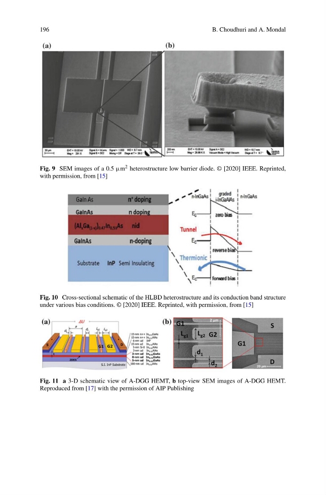
Fig. 9 SEM images of a 0.5 µm 2 heterostructure low barrier diode. © [2020] IEEE. Reprinted,
with permission, from [15]
Fig. 10 Cross-sectional schematic of the HLBD heterostructure and its conduction band structure
under various bias conditions. © [2020] IEEE. Reprinted, with permission, from [15]
Fig. 11 a 3-D schematic view of A-DGG HEMT, b top-view SEM images of A-DGG HEMT.
Reproduced from [17] with the permission of AIP Publishing
B. Choudhuri and A. Mondal
Fig. 9 SEM images of a 0.5 µm 2 heterostructure low barrier diode. © [2020] IEEE. Reprinted,
with permission, from [15]
Fig. 10 Cross-sectional schematic of the HLBD heterostructure and its conduction band structure
under various bias conditions. © [2020] IEEE. Reprinted, with permission, from [15]
Fig. 11 a 3-D schematic view of A-DGG HEMT, b top-view SEM images of A-DGG HEMT.
Reproduced from [17] with the permission of AIP Publishing