

Group III—Nitrides and Other Semiconductors for Terahertz Detector
195
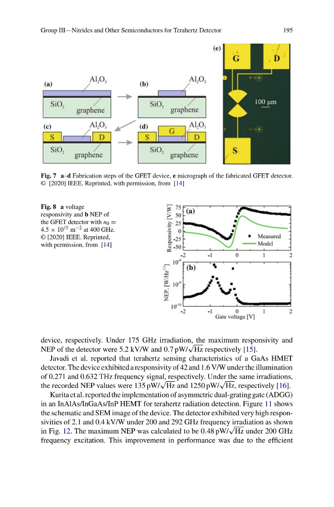
Fig. 7 a–d Fabrication steps of the GFET device, e micrograph of the fabricated GFET detector.
© [2020] IEEE. Reprinted, with permission, from [14]
Fig. 8 a voltage
responsivity and b NEP of
the GFET detector with n 0 =
4.5 × 10 15 m −2 at 400 GHz.
© [2020] IEEE. Reprinted,
with permission, from [14]
device, respectively. Under 175 GHz irradiation, the maximum responsivity and
NEP of the detector were 5.2 kV/W and 0.7 pW/
√
Hz respectively [15].
Javadi et al. reported that terahertz sensing characteristics of a GaAs HMET
detector. The device exhibited a responsivity of 42 and 1.6 V/W under the illumination
of 0.271 and 0.632 THz frequency signal, respectively. Under the same irradiations,
the recorded NEP values were 135 pW/
√
Hz and 1250 pW/
√
Hz, respectively [16].
Kurita et al. reported the implementation of asymmetric dual-grating gate (ADGG)
in an InAlAs/InGaAs/InP HEMT for terahertz radiation detection. Figure 11 shows
the schematic and SEM image of the device. The detector exhibited very high responsivities of 2.1 and 0.4 kV/W under 200 and 292 GHz frequency irradiation as shown
in Fig. 12. The maximum NEP was calculated to be 0.48 pW/
√
Hz under 200 GHz
frequency excitation. This improvement in performance was due to the efficient
195
Fig. 7 a–d Fabrication steps of the GFET device, e micrograph of the fabricated GFET detector.
© [2020] IEEE. Reprinted, with permission, from [14]
Fig. 8 a voltage
responsivity and b NEP of
the GFET detector with n 0 =
4.5 × 10 15 m −2 at 400 GHz.
© [2020] IEEE. Reprinted,
with permission, from [14]
device, respectively. Under 175 GHz irradiation, the maximum responsivity and
NEP of the detector were 5.2 kV/W and 0.7 pW/
√
Hz respectively [15].
Javadi et al. reported that terahertz sensing characteristics of a GaAs HMET
detector. The device exhibited a responsivity of 42 and 1.6 V/W under the illumination
of 0.271 and 0.632 THz frequency signal, respectively. Under the same irradiations,
the recorded NEP values were 135 pW/
√
Hz and 1250 pW/
√
Hz, respectively [16].
Kurita et al. reported the implementation of asymmetric dual-grating gate (ADGG)
in an InAlAs/InGaAs/InP HEMT for terahertz radiation detection. Figure 11 shows
the schematic and SEM image of the device. The detector exhibited very high responsivities of 2.1 and 0.4 kV/W under 200 and 292 GHz frequency irradiation as shown
in Fig. 12. The maximum NEP was calculated to be 0.48 pW/
√
Hz under 200 GHz
frequency excitation. This improvement in performance was due to the efficient