

194
B. Choudhuri and A. Mondal
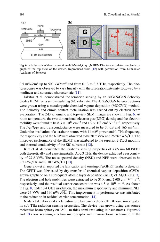
Fig. 6 a Schematic of the cross section of GaN–Al x Ga 1−x N HEMT for terahertz detection, b micrograph of the top view of the device. Reproduced from [12] with permission from Lithuanian
Academy of Sciences
0.5 mW/cm
2 up to 500 kW/cm
2 and from 0.13 to 3.3 THz, respectively. The photoresponse was observed to vary linearly with the irradiation intensity followed by a
nonlinear and saturated characteristic [11].
Jakštas et al. demonstrated the terahertz sensing by an AlGaN/GaN Schottky
diodes HEMT on a semi-insulating SiC substrate. The AlGaN/GaN heterostructures
were grown using a metalorganic chemical vapour deposition (MOCVD) method.
The Schottky and ohmic contact metallization was carried out by electron beam
evaporation. The 2-D schematic and top-view SEM images are shown in Fig. 6. At
room temperature, the two-dimensional electron gas (DEG) density and the electron
mobility were found to be 8.3 × 10
12 cm
−2 and 1.9 × 10
3 cm
2 V
−1 s
−1 , respectively.
The I ON /I OFF and transconductance were measured to be 70 dB and 165 mS/mm.
Under the irradiation of a terahertz source with 11 mW power and 0. THz frequency,
the responsivity and the NEP were observed to be 30 mV/W and 26 26 nW/
√
Hz. The
improved performance of the HEMT was attributed to the superior 2-DEG mobility
and thermal conductivity of the SiC substrate [12].
Kim et al. demonstrated the terahertz sensing properties of a 65 nm MOSFET
both theoretically and experimentally. At 0.3 THz, the device exhibited a responsivity of 27.8 V/W. The noise spectral density (NSD) and NEP were observed to be
9.5 nV/
√
Hz and 0.18 nW/
√
Hz [13].
Generalov et al. reported the fabrication and sensing of a GHET terahertz detector.
The GFET was fabricated by dry transfer of chemical vapour deposition (CVD)grown graphene on a subsequent atomic layer deposition (ALD) of Al 2 O 3 (Fig. 7).
The electron and hole mobilities were extracted to be 3100 and 2800 cm
2 V
−1 s
−1 ,
respectively, and the residual carrier concentration was 4.5 × 10
15 m
−2 . As shown
in Fig. 8, under 0.4 GHz irradiation, the maximum responsivity and minimum NEP
were 74 V/W and 130 nW/
√
Hz. This improvement in performance was attributed
to the reduction in residual carrier concentration [14].
Nadar et al. fabricated a heterostructure low barrier diode (HLBD) and investigated
its sub-THz radiation sensing properties. The device was grown using gas-source
molecular beam epitaxy on 350-µm-thick semi-insulating InP substrates. Figures 9
and 10 show scanning electron micrographs and cross-sectional schematic of the
B. Choudhuri and A. Mondal
Fig. 6 a Schematic of the cross section of GaN–Al x Ga 1−x N HEMT for terahertz detection, b micrograph of the top view of the device. Reproduced from [12] with permission from Lithuanian
Academy of Sciences
0.5 mW/cm
2 up to 500 kW/cm
2 and from 0.13 to 3.3 THz, respectively. The photoresponse was observed to vary linearly with the irradiation intensity followed by a
nonlinear and saturated characteristic [11].
Jakštas et al. demonstrated the terahertz sensing by an AlGaN/GaN Schottky
diodes HEMT on a semi-insulating SiC substrate. The AlGaN/GaN heterostructures
were grown using a metalorganic chemical vapour deposition (MOCVD) method.
The Schottky and ohmic contact metallization was carried out by electron beam
evaporation. The 2-D schematic and top-view SEM images are shown in Fig. 6. At
room temperature, the two-dimensional electron gas (DEG) density and the electron
mobility were found to be 8.3 × 10
12 cm
−2 and 1.9 × 10
3 cm
2 V
−1 s
−1 , respectively.
The I ON /I OFF and transconductance were measured to be 70 dB and 165 mS/mm.
Under the irradiation of a terahertz source with 11 mW power and 0. THz frequency,
the responsivity and the NEP were observed to be 30 mV/W and 26 26 nW/
√
Hz. The
improved performance of the HEMT was attributed to the superior 2-DEG mobility
and thermal conductivity of the SiC substrate [12].
Kim et al. demonstrated the terahertz sensing properties of a 65 nm MOSFET
both theoretically and experimentally. At 0.3 THz, the device exhibited a responsivity of 27.8 V/W. The noise spectral density (NSD) and NEP were observed to be
9.5 nV/
√
Hz and 0.18 nW/
√
Hz [13].
Generalov et al. reported the fabrication and sensing of a GHET terahertz detector.
The GFET was fabricated by dry transfer of chemical vapour deposition (CVD)grown graphene on a subsequent atomic layer deposition (ALD) of Al 2 O 3 (Fig. 7).
The electron and hole mobilities were extracted to be 3100 and 2800 cm
2 V
−1 s
−1 ,
respectively, and the residual carrier concentration was 4.5 × 10
15 m
−2 . As shown
in Fig. 8, under 0.4 GHz irradiation, the maximum responsivity and minimum NEP
were 74 V/W and 130 nW/
√
Hz. This improvement in performance was attributed
to the reduction in residual carrier concentration [14].
Nadar et al. fabricated a heterostructure low barrier diode (HLBD) and investigated
its sub-THz radiation sensing properties. The device was grown using gas-source
molecular beam epitaxy on 350-µm-thick semi-insulating InP substrates. Figures 9
and 10 show scanning electron micrographs and cross-sectional schematic of the