

192
B. Choudhuri and A. Mondal
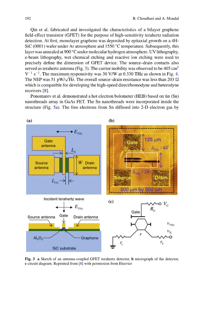
Qin et al. fabricated and investigated the characteristics of a bilayer graphene
field-effect transistor (GFET) for the purpose of high-sensitivity terahertz radiation
detection. At first, monolayer graphene was deposited by epitaxial growth on a 4HSiC (0001) wafer under Ar atmosphere and 1550 °C temperature. Subsequently, this
layer was annealed at 900 °C under molecular hydrogen atmosphere. UV lithography,
e-beam lithography, wet chemical etching and reactive ion etching were used to
precisely define the dimension of GFET device. The source–drain contacts also
served as terahertz antenna (Fig. 3). The carrier mobility was observed to be 405 cm
2
V
−1 s
−1 . The maximum responsivity was 30 V/W at 0.330 THz as shown in Fig. 4.
The NEP was 51 pW/
√
Hz. The overall source–drain resistance was less than 203
which is compatible for developing the high-speed direct/homodyne and heterodyne
receivers [8].
Ponomarev et al. demonstrated a hot electron bolometer (HEB) based on tin (Sn)
nanothreads array in GaAs FET. The Sn nanothreads were incorporated inside the
structure (Fig. 5a). The free electrons from Sn diffused into 2-D electron gas by
Fig. 3 a Sketch of an antenna-coupled GFET terahertz detector, b micrograph of the detector,
c circuit diagram. Reprinted from [8] with permission from Elsevier
B. Choudhuri and A. Mondal
Qin et al. fabricated and investigated the characteristics of a bilayer graphene
field-effect transistor (GFET) for the purpose of high-sensitivity terahertz radiation
detection. At first, monolayer graphene was deposited by epitaxial growth on a 4HSiC (0001) wafer under Ar atmosphere and 1550 °C temperature. Subsequently, this
layer was annealed at 900 °C under molecular hydrogen atmosphere. UV lithography,
e-beam lithography, wet chemical etching and reactive ion etching were used to
precisely define the dimension of GFET device. The source–drain contacts also
served as terahertz antenna (Fig. 3). The carrier mobility was observed to be 405 cm
2
V
−1 s
−1 . The maximum responsivity was 30 V/W at 0.330 THz as shown in Fig. 4.
The NEP was 51 pW/
√
Hz. The overall source–drain resistance was less than 203
which is compatible for developing the high-speed direct/homodyne and heterodyne
receivers [8].
Ponomarev et al. demonstrated a hot electron bolometer (HEB) based on tin (Sn)
nanothreads array in GaAs FET. The Sn nanothreads were incorporated inside the
structure (Fig. 5a). The free electrons from Sn diffused into 2-D electron gas by
Fig. 3 a Sketch of an antenna-coupled GFET terahertz detector, b micrograph of the detector,
c circuit diagram. Reprinted from [8] with permission from Elsevier