

Terahertz Emission Mechanisms in III–V Semiconductors …
183
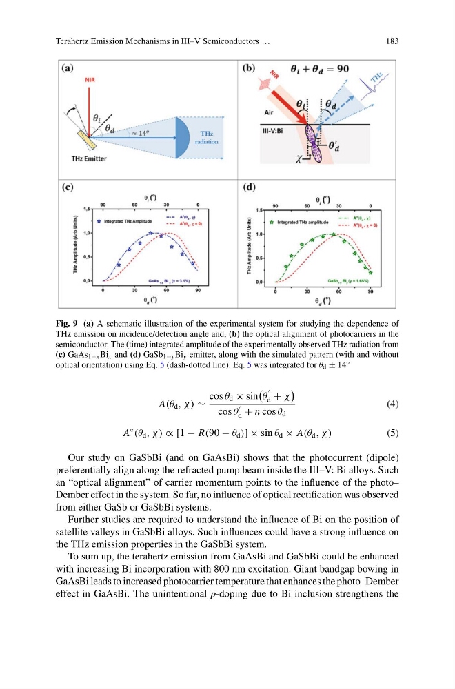
Fig. 9 (a) A schematic illustration of the experimental system for studying the dependence of
THz emission on incidence/detection angle and, (b) the optical alignment of photocarriers in the
semiconductor. The (time) integrated amplitude of the experimentally observed THz radiation from
(c) GaAs 1−x Bi x and (d) GaSb 1−y Bi y emitter, along with the simulated pattern (with and without
optical orientation) using Eq. 5 (dash-dotted line). Eq. 5 was integrated for θ d ± 14 ◦
A(θ d , χ) ∼
cos θ d × sin
θ
d + χ
cos θ
d + n cos θ d
(4)
A
◦
(θ d , χ) ∝ [1 − R(90 − θ d )] × sin θ d × A(θ d , χ)
(5)
Our study on GaSbBi (and on GaAsBi) shows that the photocurrent (dipole)
preferentially align along the refracted pump beam inside the III–V: Bi alloys. Such
an “optical alignment” of carrier momentum points to the influence of the photo–
Dember effect in the system. So far, no influence of optical rectification was observed
from either GaSb or GaSbBi systems.
Further studies are required to understand the influence of Bi on the position of
satellite valleys in GaSbBi alloys. Such influences could have a strong influence on
the THz emission properties in the GaSbBi system.
To sum up, the terahertz emission from GaAsBi and GaSbBi could be enhanced
with increasing Bi incorporation with 800 nm excitation. Giant bandgap bowing in
GaAsBi leads to increased photocarrier temperature that enhances the photo–Dember
effect in GaAsBi. The unintentional p-doping due to Bi inclusion strengthens the
183
Fig. 9 (a) A schematic illustration of the experimental system for studying the dependence of
THz emission on incidence/detection angle and, (b) the optical alignment of photocarriers in the
semiconductor. The (time) integrated amplitude of the experimentally observed THz radiation from
(c) GaAs 1−x Bi x and (d) GaSb 1−y Bi y emitter, along with the simulated pattern (with and without
optical orientation) using Eq. 5 (dash-dotted line). Eq. 5 was integrated for θ d ± 14 ◦
A(θ d , χ) ∼
cos θ d × sin
θ
d + χ
cos θ
d + n cos θ d
(4)
A
◦
(θ d , χ) ∝ [1 − R(90 − θ d )] × sin θ d × A(θ d , χ)
(5)
Our study on GaSbBi (and on GaAsBi) shows that the photocurrent (dipole)
preferentially align along the refracted pump beam inside the III–V: Bi alloys. Such
an “optical alignment” of carrier momentum points to the influence of the photo–
Dember effect in the system. So far, no influence of optical rectification was observed
from either GaSb or GaSbBi systems.
Further studies are required to understand the influence of Bi on the position of
satellite valleys in GaSbBi alloys. Such influences could have a strong influence on
the THz emission properties in the GaSbBi system.
To sum up, the terahertz emission from GaAsBi and GaSbBi could be enhanced
with increasing Bi incorporation with 800 nm excitation. Giant bandgap bowing in
GaAsBi leads to increased photocarrier temperature that enhances the photo–Dember
effect in GaAsBi. The unintentional p-doping due to Bi inclusion strengthens the