

558
T. Onodera and H. Oikawa
32.3 Resistive Switching Properties of Doped Cu-TCNQ
Nanocrystals
The resistive switching properties of doped Cu-TCNQ nanocrystals
(Cu:TCNQ=1.3:1) and bulk crystal (Cu:TCNQ=1:1) were evaluated by measuring
the current-voltage curve at room temperature. A sandwich structure was fabricated
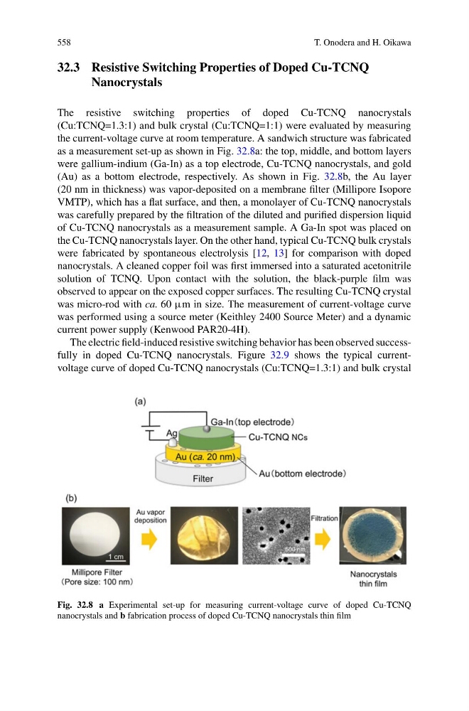
as a measurement set-up as shown in Fig. 32.8a: the top, middle, and bottom layers
were gallium-indium (Ga-In) as a top electrode, Cu-TCNQ nanocrystals, and gold
(Au) as a bottom electrode, respectively. As shown in Fig. 32.8b, the Au layer
(20 nm in thickness) was vapor-deposited on a membrane filter (Millipore Isopore
VMTP), which has a flat surface, and then, a monolayer of Cu-TCNQ nanocrystals
was carefully prepared by the filtration of the diluted and purified dispersion liquid
of Cu-TCNQ nanocrystals as a measurement sample. A Ga-In spot was placed on
the Cu-TCNQ nanocrystals layer. On the other hand, typical Cu-TCNQ bulk crystals
were fabricated by spontaneous electrolysis [12, 13] for comparison with doped
nanocrystals. A cleaned copper foil was first immersed into a saturated acetonitrile
solution of TCNQ. Upon contact with the solution, the black-purple film was
observed to appear on the exposed copper surfaces. The resulting Cu-TCNQ crystal
was micro-rod with ca. 60 µm in size. The measurement of current-voltage curve
was performed using a source meter (Keithley 2400 Source Meter) and a dynamic
current power supply (Kenwood PAR20-4H).
The electric field-induced resistive switching behavior has been observed successfully in doped Cu-TCNQ nanocrystals. Figure 32.9 shows the typical currentvoltage curve of doped Cu-TCNQ nanocrystals (Cu:TCNQ=1.3:1) and bulk crystal
Fig. 32.8 a Experimental set-up for measuring current-voltage curve of doped Cu-TCNQ
nanocrystals and b fabrication process of doped Cu-TCNQ nanocrystals thin film
T. Onodera and H. Oikawa
32.3 Resistive Switching Properties of Doped Cu-TCNQ
Nanocrystals
The resistive switching properties of doped Cu-TCNQ nanocrystals
(Cu:TCNQ=1.3:1) and bulk crystal (Cu:TCNQ=1:1) were evaluated by measuring
the current-voltage curve at room temperature. A sandwich structure was fabricated
as a measurement set-up as shown in Fig. 32.8a: the top, middle, and bottom layers
were gallium-indium (Ga-In) as a top electrode, Cu-TCNQ nanocrystals, and gold
(Au) as a bottom electrode, respectively. As shown in Fig. 32.8b, the Au layer
(20 nm in thickness) was vapor-deposited on a membrane filter (Millipore Isopore
VMTP), which has a flat surface, and then, a monolayer of Cu-TCNQ nanocrystals
was carefully prepared by the filtration of the diluted and purified dispersion liquid
of Cu-TCNQ nanocrystals as a measurement sample. A Ga-In spot was placed on
the Cu-TCNQ nanocrystals layer. On the other hand, typical Cu-TCNQ bulk crystals
were fabricated by spontaneous electrolysis [12, 13] for comparison with doped
nanocrystals. A cleaned copper foil was first immersed into a saturated acetonitrile
solution of TCNQ. Upon contact with the solution, the black-purple film was
observed to appear on the exposed copper surfaces. The resulting Cu-TCNQ crystal
was micro-rod with ca. 60 µm in size. The measurement of current-voltage curve
was performed using a source meter (Keithley 2400 Source Meter) and a dynamic
current power supply (Kenwood PAR20-4H).
The electric field-induced resistive switching behavior has been observed successfully in doped Cu-TCNQ nanocrystals. Figure 32.9 shows the typical currentvoltage curve of doped Cu-TCNQ nanocrystals (Cu:TCNQ=1.3:1) and bulk crystal
Fig. 32.8 a Experimental set-up for measuring current-voltage curve of doped Cu-TCNQ
nanocrystals and b fabrication process of doped Cu-TCNQ nanocrystals thin film