

556
T. Onodera and H. Oikawa
might be attributed to the relaxation of lattice strain loaded on Cu-TCNQ nanocrystals with an excess amount of Cu because of the large specific surface area [22].
On the other hand, Cu-TCNQ micro-rods beyond ca. 1 µm in size was the mixture
of Phases I and II from Fig. 32.4c, d. In large crystals with more ca. 1 µm in size,
the strain could be accumulated and not be released smoothly due to a relatively
smaller specific surface area. Actually, XRD peak width of nanocrystals was broader
than that of bulk crystal (Phase I) in Fig. 32.4 and became broader with increasing
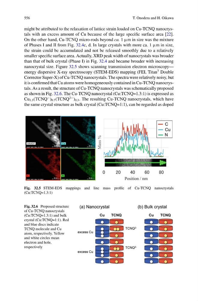
nanocrystal size. Figure 32.5 shows scanning transmission electron microscopy—
energy dispersive X-ray spectroscopy (STEM-EDS) mapping (FEI, Titan
3 Double
Corrector Super-X) of Cu-TCNQ nanocrystals. The spectra were relatively noisy, but
it is confirmed that Cu atoms were homogeneously contained in Cu-TCNQ nanocrystals. As a result, the structure of Cu-TCNQ nanocrystals was schematically proposed
as shown in Fig. 32.6. The Cu-TCNQ nanocrystal (Cu:TCNQ=1.3:1) is expressed as
Cu 1.3 (TCNQ
− ) 0.7 (TCNQ
2− ) 0.3 . The resulting Cu-TCNQ nanocrystals, which have
the same crystal structure as bulk crystal (Cu:TCNQ=1:1), can be regarded as doped
Fig. 32.5 STEM-EDS mappings and line mass profile of Cu-TCNQ nanocrystals
(Cu:TCNQ=1.3:1)
Fig. 32.6 Proposed structure
of Cu-TCNQ nanocrystals
(Cu:TCNQ=1.3:1) and bulk
crystal (Cu:TCNQ=1:1). Red
and blue discs indicate
TCNQ molecule and Cu
atom, respectively. Yellow
and white circles mean
electron and hole,
respectively
T. Onodera and H. Oikawa
might be attributed to the relaxation of lattice strain loaded on Cu-TCNQ nanocrystals with an excess amount of Cu because of the large specific surface area [22].
On the other hand, Cu-TCNQ micro-rods beyond ca. 1 µm in size was the mixture
of Phases I and II from Fig. 32.4c, d. In large crystals with more ca. 1 µm in size,
the strain could be accumulated and not be released smoothly due to a relatively
smaller specific surface area. Actually, XRD peak width of nanocrystals was broader
than that of bulk crystal (Phase I) in Fig. 32.4 and became broader with increasing
nanocrystal size. Figure 32.5 shows scanning transmission electron microscopy—
energy dispersive X-ray spectroscopy (STEM-EDS) mapping (FEI, Titan
3 Double
Corrector Super-X) of Cu-TCNQ nanocrystals. The spectra were relatively noisy, but
it is confirmed that Cu atoms were homogeneously contained in Cu-TCNQ nanocrystals. As a result, the structure of Cu-TCNQ nanocrystals was schematically proposed
as shown in Fig. 32.6. The Cu-TCNQ nanocrystal (Cu:TCNQ=1.3:1) is expressed as
Cu 1.3 (TCNQ
− ) 0.7 (TCNQ
2− ) 0.3 . The resulting Cu-TCNQ nanocrystals, which have
the same crystal structure as bulk crystal (Cu:TCNQ=1:1), can be regarded as doped
Fig. 32.5 STEM-EDS mappings and line mass profile of Cu-TCNQ nanocrystals
(Cu:TCNQ=1.3:1)
Fig. 32.6 Proposed structure
of Cu-TCNQ nanocrystals
(Cu:TCNQ=1.3:1) and bulk
crystal (Cu:TCNQ=1:1). Red
and blue discs indicate
TCNQ molecule and Cu
atom, respectively. Yellow
and white circles mean
electron and hole,
respectively