

32 Fabrication of Charge-Transfer Complex Nanocrystals …
555
the chemical state of Cu in Cu-TCNQ nanocrystals was mono cation. Actually, it
is reported that the main peaks for the Cu-L 3 edge are located at 935.5 eV for Cu,
936.1 eV for Cu 2 O, 933.6 eV for CuO, respectively [21]. These facts demonstrate
that the excess amount of Cu resulted in the generation of TCNQ dianions in CuTCNQ nanocrystals to keep the charge balance between TCNQ and excessive Cu.
Moreover, it is noted that the Raman intensity ratio of dianion (C=C stretching mode
at 1320 nm) to anion (C=C ring stretching mode at 1380 nm) increased as crystal
size increased [17]. This fact suggests that the degree of charge-transfer γ from Cu
to TCNQ in nanocrystals would be dependent on crystal size.
Next, crystal structure of Cu-TCNQ nanocrystals was examined by measuring
powder X-ray diffraction (XRD) patterns (Bruker, D8 Advance). It is reported that
Cu-TCNQ crystal has two polymorphic forms [19]. Phase I has a face-to-face packing
structure, in which planar TCNQ molecules are stacked with effective π-π interaction
between adjacent TCNQ molecules. The other is phase II with high resistance, which
has a tetragonal structure. In a viewpoint of electronic device application, phase I is
a very important material because of unique switching behavior between complete
and partial charge-transfer states by applying electric field and/or irradiating light
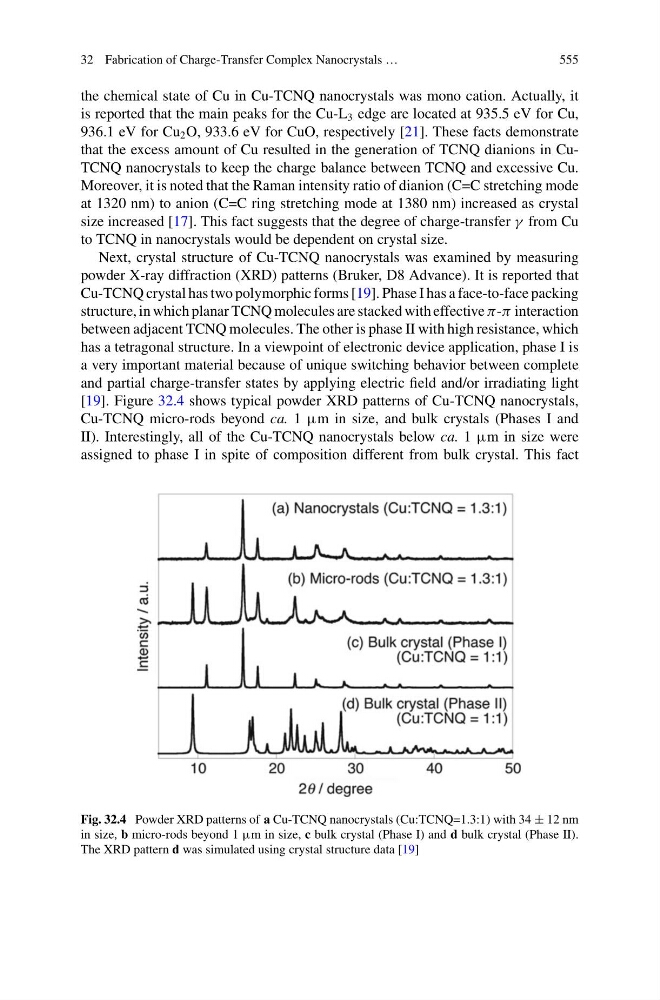
[19]. Figure 32.4 shows typical powder XRD patterns of Cu-TCNQ nanocrystals,
Cu-TCNQ micro-rods beyond ca. 1 µm in size, and bulk crystals (Phases I and
II). Interestingly, all of the Cu-TCNQ nanocrystals below ca. 1 µm in size were
assigned to phase I in spite of composition different from bulk crystal. This fact
Fig. 32.4 Powder XRD patterns of a Cu-TCNQ nanocrystals (Cu:TCNQ=1.3:1) with 34 ± 12 nm
in size, b micro-rods beyond 1 µm in size, c bulk crystal (Phase I) and d bulk crystal (Phase II).
The XRD pattern d was simulated using crystal structure data [19]
555
the chemical state of Cu in Cu-TCNQ nanocrystals was mono cation. Actually, it
is reported that the main peaks for the Cu-L 3 edge are located at 935.5 eV for Cu,
936.1 eV for Cu 2 O, 933.6 eV for CuO, respectively [21]. These facts demonstrate
that the excess amount of Cu resulted in the generation of TCNQ dianions in CuTCNQ nanocrystals to keep the charge balance between TCNQ and excessive Cu.
Moreover, it is noted that the Raman intensity ratio of dianion (C=C stretching mode
at 1320 nm) to anion (C=C ring stretching mode at 1380 nm) increased as crystal
size increased [17]. This fact suggests that the degree of charge-transfer γ from Cu
to TCNQ in nanocrystals would be dependent on crystal size.
Next, crystal structure of Cu-TCNQ nanocrystals was examined by measuring
powder X-ray diffraction (XRD) patterns (Bruker, D8 Advance). It is reported that
Cu-TCNQ crystal has two polymorphic forms [19]. Phase I has a face-to-face packing
structure, in which planar TCNQ molecules are stacked with effective π-π interaction
between adjacent TCNQ molecules. The other is phase II with high resistance, which
has a tetragonal structure. In a viewpoint of electronic device application, phase I is
a very important material because of unique switching behavior between complete
and partial charge-transfer states by applying electric field and/or irradiating light
[19]. Figure 32.4 shows typical powder XRD patterns of Cu-TCNQ nanocrystals,
Cu-TCNQ micro-rods beyond ca. 1 µm in size, and bulk crystals (Phases I and
II). Interestingly, all of the Cu-TCNQ nanocrystals below ca. 1 µm in size were
assigned to phase I in spite of composition different from bulk crystal. This fact
Fig. 32.4 Powder XRD patterns of a Cu-TCNQ nanocrystals (Cu:TCNQ=1.3:1) with 34 ± 12 nm
in size, b micro-rods beyond 1 µm in size, c bulk crystal (Phase I) and d bulk crystal (Phase II).
The XRD pattern d was simulated using crystal structure data [19]