

13 Controlling Optical Properties of Multinary Quantum Dots …
227
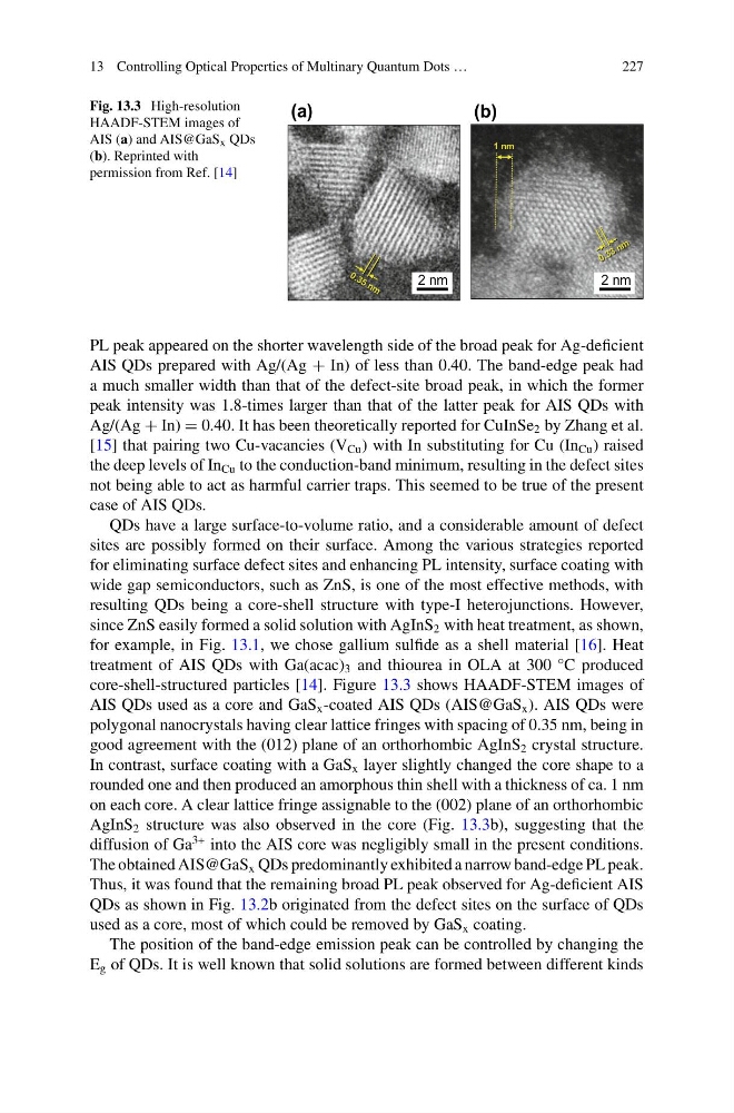
Fig. 13.3 High-resolution
HAADF-STEM images of
AIS (a) and AIS@GaS x QDs
(b). Reprinted with
permission from Ref. [14]
(b)
2 nm
(a)
2 nm
1 nm
PL peak appeared on the shorter wavelength side of the broad peak for Ag-deficient
AIS QDs prepared with Ag/(Ag + In) of less than 0.40. The band-edge peak had
a much smaller width than that of the defect-site broad peak, in which the former
peak intensity was 1.8-times larger than that of the latter peak for AIS QDs with
Ag/(Ag + In) = 0.40. It has been theoretically reported for CuInSe 2 by Zhang et al.
[15] that pairing two Cu-vacancies (V Cu ) with In substituting for Cu (In Cu ) raised
the deep levels of In Cu to the conduction-band minimum, resulting in the defect sites
not being able to act as harmful carrier traps. This seemed to be true of the present
case of AIS QDs.
QDs have a large surface-to-volume ratio, and a considerable amount of defect
sites are possibly formed on their surface. Among the various strategies reported
for eliminating surface defect sites and enhancing PL intensity, surface coating with
wide gap semiconductors, such as ZnS, is one of the most effective methods, with
resulting QDs being a core-shell structure with type-I heterojunctions. However,
since ZnS easily formed a solid solution with AgInS 2 with heat treatment, as shown,
for example, in Fig. 13.1, we chose gallium sulfide as a shell material [16]. Heat
treatment of AIS QDs with Ga(acac) 3 and thiourea in OLA at 300 °C produced
core-shell-structured particles [14]. Figure 13.3 shows HAADF-STEM images of
AIS QDs used as a core and GaS x -coated AIS QDs (AIS@GaS x ). AIS QDs were
polygonal nanocrystals having clear lattice fringes with spacing of 0.35 nm, being in
good agreement with the (012) plane of an orthorhombic AgInS 2 crystal structure.
In contrast, surface coating with a GaS x layer slightly changed the core shape to a
rounded one and then produced an amorphous thin shell with a thickness of ca. 1 nm
on each core. A clear lattice fringe assignable to the (002) plane of an orthorhombic
AgInS 2 structure was also observed in the core (Fig. 13.3b), suggesting that the
diffusion of Ga
3+ into the AIS core was negligibly small in the present conditions.
The obtained AIS@GaS x QDs predominantly exhibited a narrow band-edge PL peak.
Thus, it was found that the remaining broad PL peak observed for Ag-deficient AIS
QDs as shown in Fig. 13.2b originated from the defect sites on the surface of QDs
used as a core, most of which could be removed by GaS x coating.
The position of the band-edge emission peak can be controlled by changing the
E g of QDs. It is well known that solid solutions are formed between different kinds
227
Fig. 13.3 High-resolution
HAADF-STEM images of
AIS (a) and AIS@GaS x QDs
(b). Reprinted with
permission from Ref. [14]
(b)
2 nm
(a)
2 nm
1 nm
PL peak appeared on the shorter wavelength side of the broad peak for Ag-deficient
AIS QDs prepared with Ag/(Ag + In) of less than 0.40. The band-edge peak had
a much smaller width than that of the defect-site broad peak, in which the former
peak intensity was 1.8-times larger than that of the latter peak for AIS QDs with
Ag/(Ag + In) = 0.40. It has been theoretically reported for CuInSe 2 by Zhang et al.
[15] that pairing two Cu-vacancies (V Cu ) with In substituting for Cu (In Cu ) raised
the deep levels of In Cu to the conduction-band minimum, resulting in the defect sites
not being able to act as harmful carrier traps. This seemed to be true of the present
case of AIS QDs.
QDs have a large surface-to-volume ratio, and a considerable amount of defect
sites are possibly formed on their surface. Among the various strategies reported
for eliminating surface defect sites and enhancing PL intensity, surface coating with
wide gap semiconductors, such as ZnS, is one of the most effective methods, with
resulting QDs being a core-shell structure with type-I heterojunctions. However,
since ZnS easily formed a solid solution with AgInS 2 with heat treatment, as shown,
for example, in Fig. 13.1, we chose gallium sulfide as a shell material [16]. Heat
treatment of AIS QDs with Ga(acac) 3 and thiourea in OLA at 300 °C produced
core-shell-structured particles [14]. Figure 13.3 shows HAADF-STEM images of
AIS QDs used as a core and GaS x -coated AIS QDs (AIS@GaS x ). AIS QDs were
polygonal nanocrystals having clear lattice fringes with spacing of 0.35 nm, being in
good agreement with the (012) plane of an orthorhombic AgInS 2 crystal structure.
In contrast, surface coating with a GaS x layer slightly changed the core shape to a
rounded one and then produced an amorphous thin shell with a thickness of ca. 1 nm
on each core. A clear lattice fringe assignable to the (002) plane of an orthorhombic
AgInS 2 structure was also observed in the core (Fig. 13.3b), suggesting that the
diffusion of Ga
3+ into the AIS core was negligibly small in the present conditions.
The obtained AIS@GaS x QDs predominantly exhibited a narrow band-edge PL peak.
Thus, it was found that the remaining broad PL peak observed for Ag-deficient AIS
QDs as shown in Fig. 13.2b originated from the defect sites on the surface of QDs
used as a core, most of which could be removed by GaS x coating.
The position of the band-edge emission peak can be controlled by changing the
E g of QDs. It is well known that solid solutions are formed between different kinds