

P1 is initialized at the start of the instruction execution; P2 is required and
initiated when fault has been detected, but it is essential that the pre-modified state
is stored at the start of execution of every instruction. P1 and P3 can operate
concurrently.
P1 and P2 have an influence on each other: the higher the fault detection coverage achieved by P1, the more successful recovery should be.
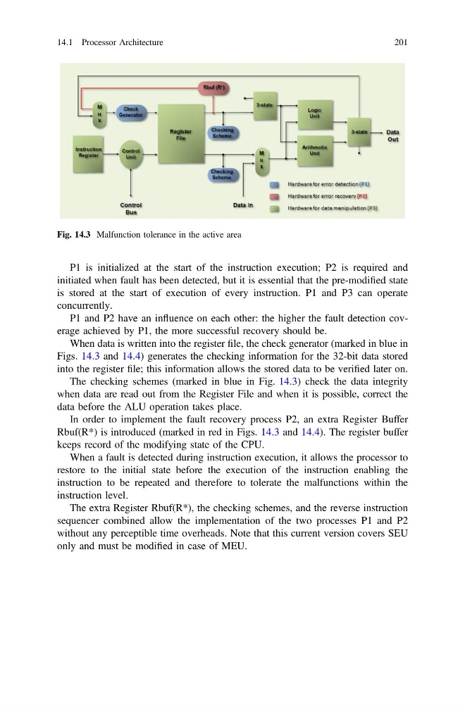
When data is written into the register file, the check generator (marked in blue in
Figs. 14.3 and 14.4) generates the checking information for the 32-bit data stored
into the register file; this information allows the stored data to be verified later on.
The checking schemes (marked in blue in Fig. 14.3) check the data integrity
when data are read out from the Register File and when it is possible, correct the
data before the ALU operation takes place.
In order to implement the fault recovery process P2, an extra Register Buffer
Rbuf(R*) is introduced (marked in red in Figs. 14.3 and 14.4). The register buffer
keeps record of the modifying state of the CPU.
When a fault is detected during instruction execution, it allows the processor to
restore to the initial state before the execution of the instruction enabling the
instruction to be repeated and therefore to tolerate the malfunctions within the
instruction level.
The extra Register Rbuf(R*), the checking schemes, and the reverse instruction
sequencer combined allow the implementation of the two processes P1 and P2
without any perceptible time overheads. Note that this current version covers SEU
only and must be modified in case of MEU.
Fig. 14.3 Malfunction tolerance in the active area
14.1 Processor Architecture
201
initiated when fault has been detected, but it is essential that the pre-modified state
is stored at the start of execution of every instruction. P1 and P3 can operate
concurrently.
P1 and P2 have an influence on each other: the higher the fault detection coverage achieved by P1, the more successful recovery should be.
When data is written into the register file, the check generator (marked in blue in
Figs. 14.3 and 14.4) generates the checking information for the 32-bit data stored
into the register file; this information allows the stored data to be verified later on.
The checking schemes (marked in blue in Fig. 14.3) check the data integrity
when data are read out from the Register File and when it is possible, correct the
data before the ALU operation takes place.
In order to implement the fault recovery process P2, an extra Register Buffer
Rbuf(R*) is introduced (marked in red in Figs. 14.3 and 14.4). The register buffer
keeps record of the modifying state of the CPU.
When a fault is detected during instruction execution, it allows the processor to
restore to the initial state before the execution of the instruction enabling the
instruction to be repeated and therefore to tolerate the malfunctions within the
instruction level.
The extra Register Rbuf(R*), the checking schemes, and the reverse instruction
sequencer combined allow the implementation of the two processes P1 and P2
without any perceptible time overheads. Note that this current version covers SEU
only and must be modified in case of MEU.
Fig. 14.3 Malfunction tolerance in the active area
14.1 Processor Architecture
201