

Characterization Techniques in Nanotechnology …
51
an STM image representing the surface topography. The STM has capacity for three
functions which are surface imaging, tunneling spectroscopy, and tip manipulation.
STM has been deployed in numerous research studies such as semiconductor
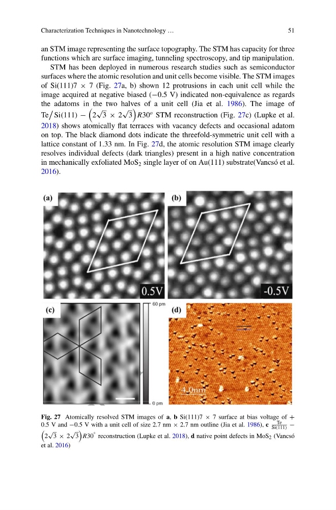
surfaces where the atomic resolution and unit cells become visible. The STM images
of Si(111)7 × 7 (Fig. 27a, b) shown 12 protrusions in each unit cell while the
image acquired at negative biased (−0.5 V) indicated non-equivalence as regards
the adatoms in the two halves of a unit cell (Jia et al. 1986). The image of
Te
Si(111) −
2
√
3 × 2
√
3
R30
o STM reconstruction (Fig. 27c) (Lupke et al.
2018) shows atomically flat terraces with vacancy defects and occasional adatom
on top. The black diamond dots indicate the threefold-symmetric unit cell with a
lattice constant of 1.33 nm. In Fig. 27d, the atomic resolution STM image clearly
resolves individual defects (dark triangles) present in a high native concentration
in mechanically exfoliated MoS 2 single layer of on Au(111) substrate(Vancsó et al.
2016).
Fig. 27 Atomically resolved STM images of a, b Si(111)7 × 7 surface at bias voltage of +
0.5 V and −0.5 V with a unit cell of size 2.7 nm × 2.7 nm outline (Jia et al. 1986), c
Te
Si(111) −
2
√
3 × 2
√
3
R30
◦ reconstruction (Lupke et al. 2018), d native point defects in MoS 2 (Vancsó
et al. 2016)
51
an STM image representing the surface topography. The STM has capacity for three
functions which are surface imaging, tunneling spectroscopy, and tip manipulation.
STM has been deployed in numerous research studies such as semiconductor
surfaces where the atomic resolution and unit cells become visible. The STM images
of Si(111)7 × 7 (Fig. 27a, b) shown 12 protrusions in each unit cell while the
image acquired at negative biased (−0.5 V) indicated non-equivalence as regards
the adatoms in the two halves of a unit cell (Jia et al. 1986). The image of
Te
Si(111) −
2
√
3 × 2
√
3
R30
o STM reconstruction (Fig. 27c) (Lupke et al.
2018) shows atomically flat terraces with vacancy defects and occasional adatom
on top. The black diamond dots indicate the threefold-symmetric unit cell with a
lattice constant of 1.33 nm. In Fig. 27d, the atomic resolution STM image clearly
resolves individual defects (dark triangles) present in a high native concentration
in mechanically exfoliated MoS 2 single layer of on Au(111) substrate(Vancsó et al.
2016).
Fig. 27 Atomically resolved STM images of a, b Si(111)7 × 7 surface at bias voltage of +
0.5 V and −0.5 V with a unit cell of size 2.7 nm × 2.7 nm outline (Jia et al. 1986), c
Te
Si(111) −
2
√
3 × 2
√
3
R30
◦ reconstruction (Lupke et al. 2018), d native point defects in MoS 2 (Vancsó
et al. 2016)