

50
T. B. Asafa et al.
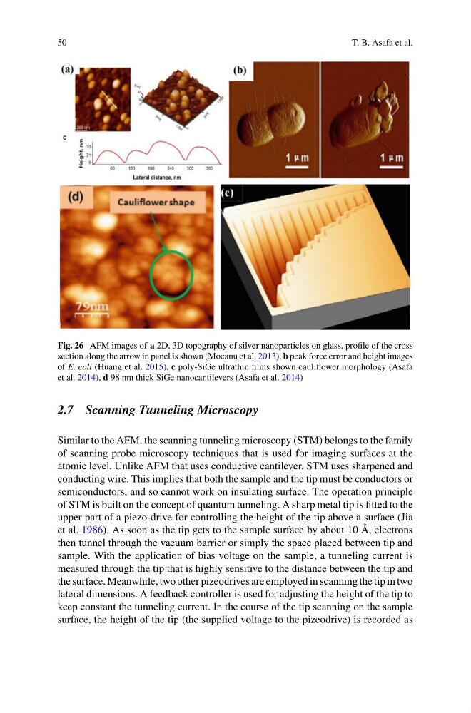
Fig. 26 AFM images of a 2D, 3D topography of silver nanoparticles on glass, profile of the cross
section along the arrow in panel is shown (Mocanu et al. 2013), b peak force error and height images
of E. coli (Huang et al. 2015), c poly-SiGe ultrathin films shown cauliflower morphology (Asafa
et al. 2014), d 98 nm thick SiGe nanocantilevers (Asafa et al. 2014)
2.7 Scanning Tunneling Microscopy
Similar to the AFM, the scanning tunneling microscopy (STM) belongs to the family
of scanning probe microscopy techniques that is used for imaging surfaces at the
atomic level. Unlike AFM that uses conductive cantilever, STM uses sharpened and
conducting wire. This implies that both the sample and the tip must be conductors or
semiconductors, and so cannot work on insulating surface. The operation principle
of STM is built on the concept of quantum tunneling. A sharp metal tip is fitted to the
upper part of a piezo-drive for controlling the height of the tip above a surface (Jia
et al. 1986). As soon as the tip gets to the sample surface by about 10 Å, electrons
then tunnel through the vacuum barrier or simply the space placed between tip and
sample. With the application of bias voltage on the sample, a tunneling current is
measured through the tip that is highly sensitive to the distance between the tip and
the surface. Meanwhile, two other pizeodrives are employed in scanning the tip in two
lateral dimensions. A feedback controller is used for adjusting the height of the tip to
keep constant the tunneling current. In the course of the tip scanning on the sample
surface, the height of the tip (the supplied voltage to the pizeodrive) is recorded as
T. B. Asafa et al.
Fig. 26 AFM images of a 2D, 3D topography of silver nanoparticles on glass, profile of the cross
section along the arrow in panel is shown (Mocanu et al. 2013), b peak force error and height images
of E. coli (Huang et al. 2015), c poly-SiGe ultrathin films shown cauliflower morphology (Asafa
et al. 2014), d 98 nm thick SiGe nanocantilevers (Asafa et al. 2014)
2.7 Scanning Tunneling Microscopy
Similar to the AFM, the scanning tunneling microscopy (STM) belongs to the family
of scanning probe microscopy techniques that is used for imaging surfaces at the
atomic level. Unlike AFM that uses conductive cantilever, STM uses sharpened and
conducting wire. This implies that both the sample and the tip must be conductors or
semiconductors, and so cannot work on insulating surface. The operation principle
of STM is built on the concept of quantum tunneling. A sharp metal tip is fitted to the
upper part of a piezo-drive for controlling the height of the tip above a surface (Jia
et al. 1986). As soon as the tip gets to the sample surface by about 10 Å, electrons
then tunnel through the vacuum barrier or simply the space placed between tip and
sample. With the application of bias voltage on the sample, a tunneling current is
measured through the tip that is highly sensitive to the distance between the tip and
the surface. Meanwhile, two other pizeodrives are employed in scanning the tip in two
lateral dimensions. A feedback controller is used for adjusting the height of the tip to
keep constant the tunneling current. In the course of the tip scanning on the sample
surface, the height of the tip (the supplied voltage to the pizeodrive) is recorded as